HSP50216(2000) 데이터 시트보기 (PDF) - Intersil
부품명
상세내역
제조사
HSP50216 Datasheet PDF : 53 Pages
| |||
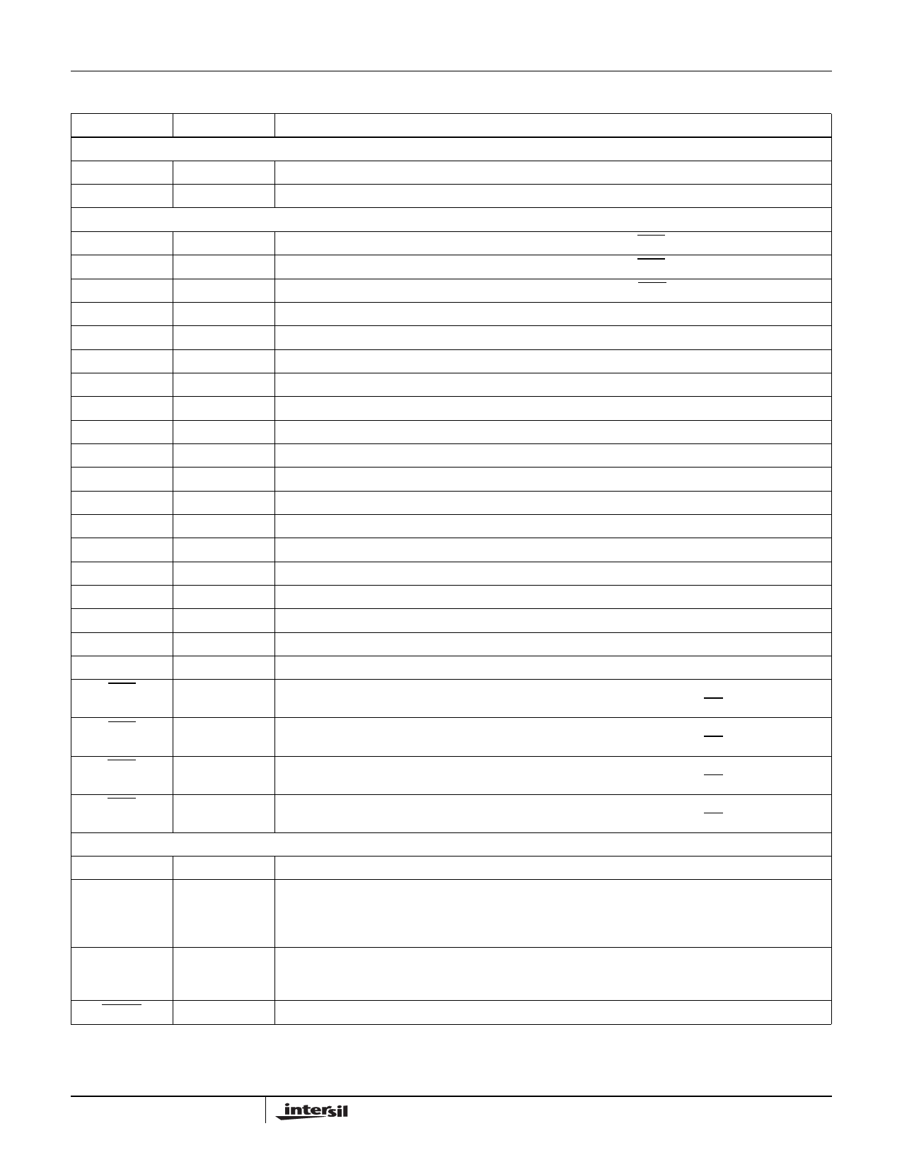
Pin Descriptions
NAME
POWER SUPPLY
VCC
GND
INPUTS
A(15:0)
B(15:0)
C(15:0)
D(15:0)
ENIA
TYPE
-
-
I
I
I
I
I
ENIB
I
ENIC
I
ENID
I
CONTROL
CLK
I
SYNCI
I
SYNCO
O
RESET
I
OUTPUTS
SD1A
O
SD2A
O
SD1B
O
SD2B
O
SD1C
O
SD2C
O
SD1D
O
SD2D
O
SCLK
O
SYNCA
O
HSP50216
DESCRIPTION
Positive Power Supply Voltage, 3.3V ±0.15
Ground, 0V.
Parallel Data Input bus A. Sampled on the rising edge of clock when ENIA is active (low).
Parallel Data Input bus B. Sampled on the rising edge of clock when ENIB is active (low).
Parallel Data Input bus C. Sampled on the rising edge of clock when ENIC is active (low).
Parallel Data Input bus D. Sampled on the rising edge of clock when ENID is active (low).
Input enable for Parallel Data Input bus A. Active low. This pin enables the input to the part in one of two
modes, gated or interpolated. In gated mode, one sample is taken per CLK when ENI is asserted.
Input enable for Parallel Data Input bus B. Active low. This pin enables the input to the part in one of two
modes, gated or interpolated. In gated mode, one sample is taken per CLK when ENI is asserted.
Input enable for Parallel Data Input bus C. Active low. This pin enables the input to the part in one of two
modes, gated or interpolated. In gated mode, one sample is taken per CLK when ENI is asserted.
Input enable for Parallel Data Input bus D. Active low. This pin enables the input to the part in one of two
modes, gated or interpolated. In gated mode, one sample is taken per CLK when ENI is asserted.
Input clock. All processing in the HSP50216 occurs on the rising edge of CLK.
Synchronization Input Signal. Used to align the processing with an external event or with other HSP50216
devices. SYNCI can update the carrier NCO, reset decimation counters, restart the filter compute engine,
and restart the output section among other functions. For most of the functional blocks, the response to
SYNCI is programmable and can be enabled or disabled.
Synchronization Output Signal. The processing of multiple HSP50216 devices can be synchronized by
tying the SYNCO from one HSP50216 device (the master) to the SYNCI of all the HSP50216 devices (the
master and slaves).
Reset Signal. Active low. Asserting reset will halt all processing and set certain registers to default values.
Serial Data Output 1A. A serial data stream output which can be programmed to consist of I1, Q1, I2, Q2,
magnitude, phase, frequency (dφ/dt), AGC gain, and/or zeros. In addition, data outputs from Channels 0,
1, 2 and 3 can be multiplexed into a common serial output data stream. Information can be sequenced in
a programmable order. See Serial Data Output Formatter Section and Microprocessor Interface Section.
Serial Data Output 2A. This output is provided as an auxiliary output for Serial Data Output 1A to route data
to a second destination or to output two words at a time for higher sample rates. SD2A has the same
programmability as SD1A except that floating point format is not available. See Serial Data Output
Formatter Section and Microprocessor Interface Section.
Serial Data Output 1B. See description for SD1A.
Serial Data Output 2B. See description for SD2A.
Serial Data Output 1C. See description for SD1A.
Serial Data Output 2C. See description for SD2A.
Serial Data Output 1D. See description for SD1A.
Serial Data Output 2D. See description for SD2A.
Serial Output Clock. Can be programmed to be at 1, 1/2, 1/4, 1/8, or 1/16 times the clock frequency. The
polarity of SCLK is programmable.
Serial Data Output 1A sync signal. This signal is used to indicate the start of a data word and/or frame of
data. The polarity and position of SYNCA is programmable.
4
Share Link: 