AA090MF01--T1 데이터 시트보기 (PDF) - Unspecified
부품명
상세내역
제조사
AA090MF01--T1 Datasheet PDF : 29 Pages
| |||
5. INTERFACE PIN CONNECTION
(1) CN 1(Interface Signal)
Used connector: FI-SE20P-HFE (JAE)
Corresponding connector: FI-S20S [for discrete Wire], FI-SE20ME [for FPC] (JAE)
Pin
No.
Symbol
Function (ISP 6 bit compatibility mode)
6 bit input
8 bit input
Function (ISP 8 bit
compatibility mode)
1 VCC
+3.3 V Power supply
←
2 VCC
+3.3 V Power supply
←
3 GND
GND
←
4 GND
GND
←
5 Link 0− R0, R1, R2, R3, R4, R5, G0 R2, R3, R4, R5, R6, R7, G2 R0, R1, R2, R3, R4, R5, G0
6 Link 0+ R0, R1, R2, R3, R4, R5, G0 R2, R3, R4, R5, R6, R7, G2 R0, R1, R2, R3, R4, R5, G0
7 GND
GND
←
8 Link 1− G1, G2, G3, G4, G5, B0, B1 G3, G4, G5, G6, G7, B2, B3 G1, G2, G3, G4, G5, B0, B1
9 Link 1+ G1, G2, G3, G4, G5, B0, B1 G3, G4, G5, G6, G7, B2, B3 G1, G2, G3, G4, G5, B0, B1
10 GND
GND
←
11 Link 2− B2, B3, B4, B5, DENA
B4, B5, B6, B7, DENA
B2, B3, B4, B5, DENA
12 Link 2+ B2, B3, B4, B5, DENA
B4, B5, B6, B7, DENA
B2, B3, B4, B5, DENA
13 GND
GND
←
14 CLKIN−
Clock −
←
15 CLKIN+
Clock +
←
16 GND
GND
←
17 Link3− See: *2)
R0, R1, G0, G1, B0, B1
R6, R7, G6, G7, B6, B7
18 Link3+ See: *2)
R0, R1, G0, G1, B0, B1
R6, R7, G6, G7, B6, B7
19 MODE
Low=ISP 6 bit compatibility mode
High=ISP
8 bit compatibility mode
20 SC
Scan direction control (Low=Normal, High=Reverse) ←
*1) Metal frame is connected to signal GND.
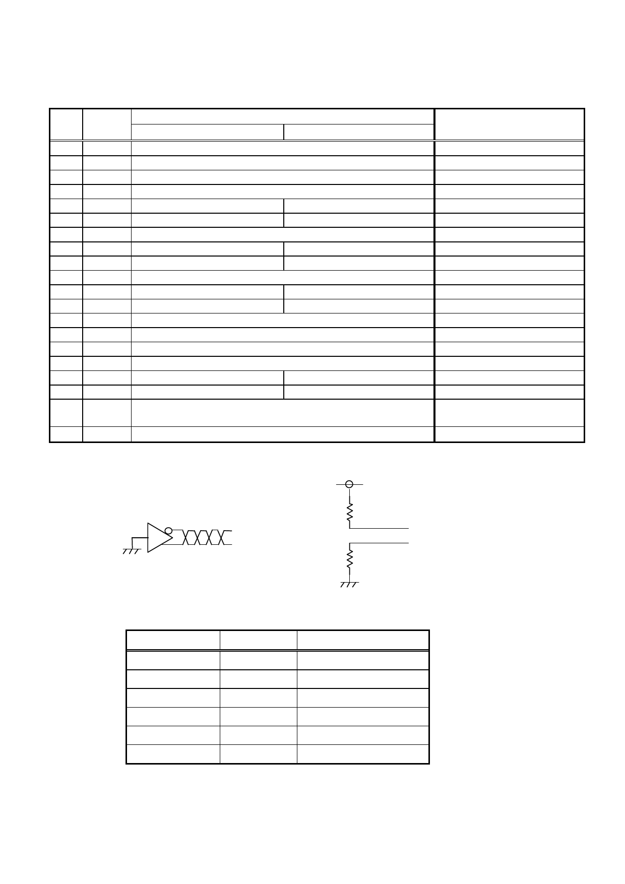
*2) Recommended wiring of Pin 17,18 (6 bit input)
VCC
LVDS
transmitter
LOW data
Pin 17
680 Ω
Pin 17
Pin 18
or
Pin 18
620 Ω
(2) CN 2(Backlight)
Backlight-side connector: SM06B-SHLS-TF(LF)(SN) (JST)
Corresponding connector: SHLP-06V-S-B (JST)
Pin No.
Symbol
Function
1
NC
This pin should be open.
2
NC
This pin should be open.
3
LED C 1
LED cathode 1
4
LED A 1
LED anode 1
5
LED A 2
LED anode 2
6
LED C 2
LED cathode 2
MITSUBISHI
(8/29)
AA090MF01--T1_02_00
Share Link: 