CXA2040 데이터 시트보기 (PDF) - Sony Semiconductor
부품명
상세내역
제조사
CXA2040 Datasheet PDF : 22 Pages
| |||
CXA2040Q
2) Status Register
S Slave address A DATA NA P
S: START CONDITION
P: STOP CONDITION
A: ACKNOWLEDGE
• Slave address
100100X1
R/W bit
This bit is set to "1" when data is to be read into the status
registers.
Value set by the address pin
DATA
bit7
PON
RES
bit6 bit5 bit4 bit3 bit2 bit1 bit0
X
SYNC
SEP
X
S1
S1 S2
S2
OPEN SEL OPEN SEL
(1) PONRES
Returns "1" when the CXA2040Q is POWER ON RESET. Becomes "0" after reading once.
(2) SYNCSEP
"1" returns if sync exists, "0" if sync does not exist.
(3) OPEN/SEL for S1 and S2 is determined by comparing the DC voltages for S1 and S2 pins with two
threshold levels.
DC voltages for S1 and S2 pins S1, S2 OPEN S1, S2 SEL
2V or less
0
1
4.75 to 7.25V
0
0
9.5 to 12V
1
0
3) POWER ON RESET
The CXA2040Q incorporates a POWER ON RESET function which sets each control register to "0" upon
POWER ON. (Which goes to MUTE status.)
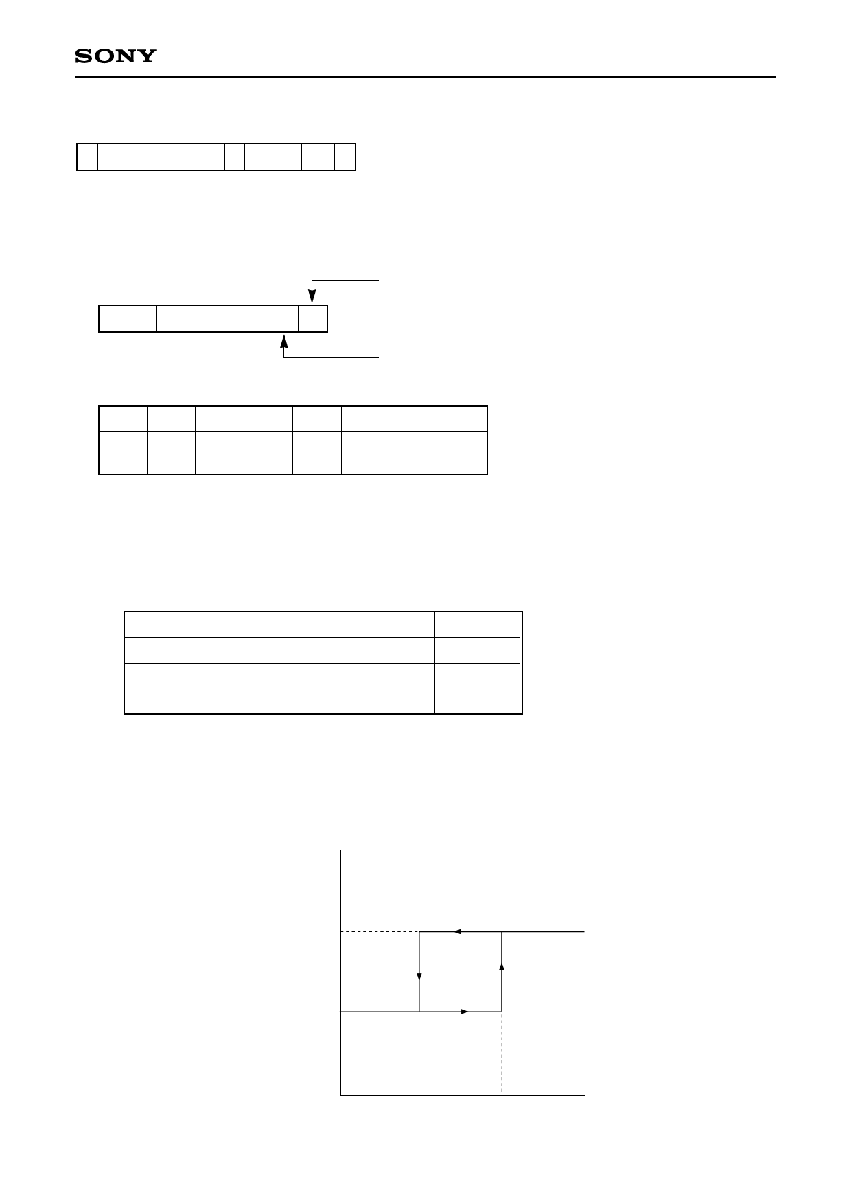
The POWER ON RESET VTH has hysteresis. The POWER ON VCC and released VCC are as shown below.
Also, the PONRES bit of the status register is read to determine whether the IC is reset upon POWER ON.
POWER ON RESET RELEASE
POWER ON RESET
Vcc
4.7V
5.9V
– 16 –
Share Link: 