CXA2040 데이터 시트보기 (PDF) - Sony Semiconductor
부품명
상세내역
제조사
CXA2040 Datasheet PDF : 22 Pages
| |||
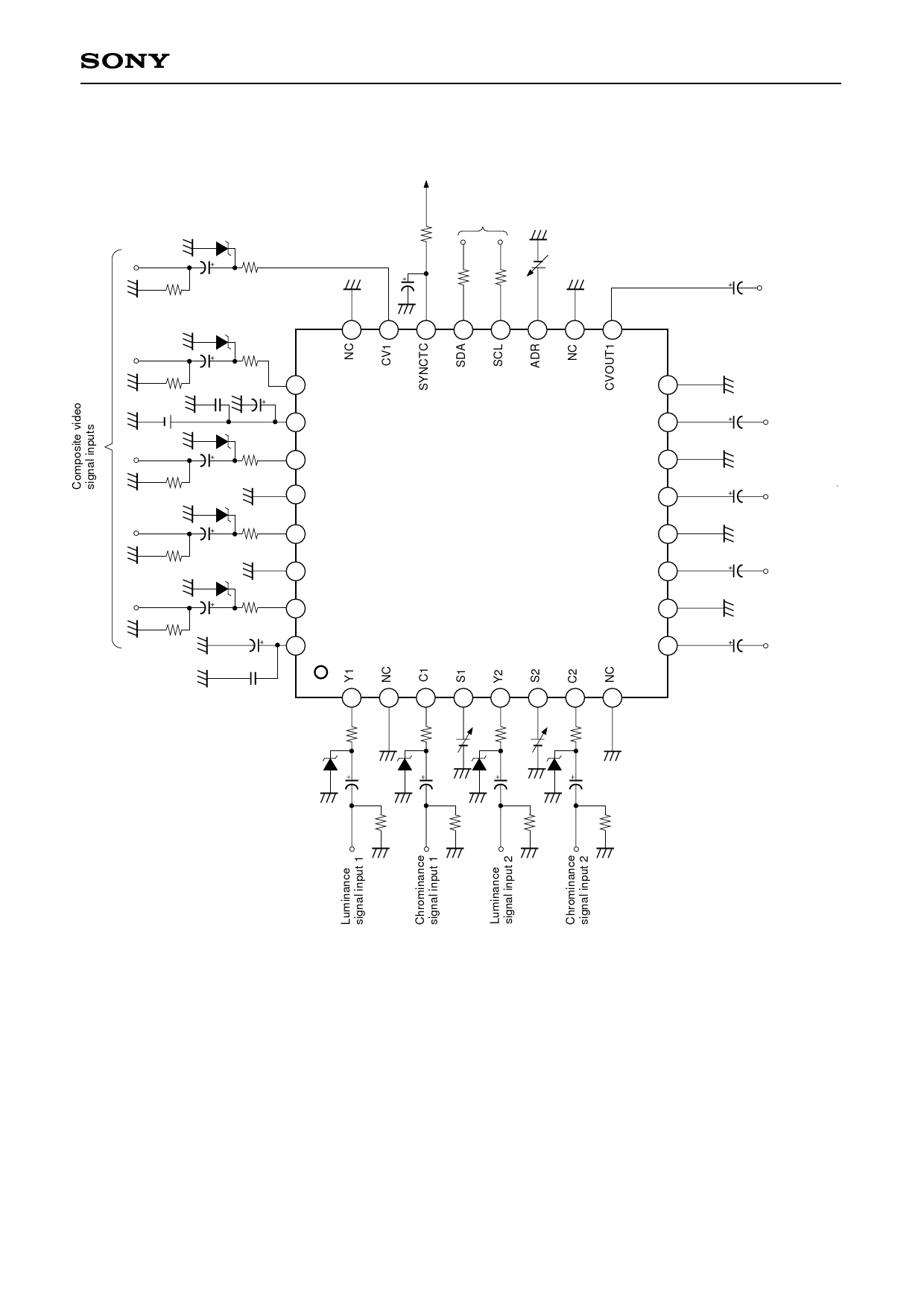
CXA2040Q
Application Circuit
VCC
2.2µ 220
75
I2C BUS
68k
0.1µ
220 220
VADR
24 23 22 21 20 19 18 17
2.2µ 220
75 0.01µ 33µ
Vcc
9V
2.2µ 220
75
25 CV2
26 VCC
27 CV3
28 NC
2.2µ 220
75
29 CV4
30 GND
2.2µ
75
220
33µ
31 CV5
32 BIAS
0.01µ
1
2
220
CXA2040Q
NC 16
CVOUT2 15
NC 14
CVOUT3 13
NC 12
YOUT 11
NC 10
COUT 9
3
4
5
6
7
8
Vs1
Vs2
220
220
220
2.2µ
75
2.2µ
75
2.2µ
75
2.2µ
75
Composite
video signal
10µ 0dB output 1
Composite
video signal
10µ +6dB output 2
Composite
video signal
10µ 0dB output 3
Luminance
signal output
10µ
0.47µ
Chrominance
signal output
∗1 Input pins of Pins 1, 3, 5, 7, 23, 25, 27, 29 and 31 are biased to approximately 4.2 to 4.7V. Therefore, care
should be taken for the capacitance polarity.
∗2 Output pins of Pins 9, 11, 13, 15 and 17 are biased to approximately 3.8 to 4.8V. Therefore, care should be
taken for the capacitance polarity.
∗3 Set VADR to 0V (GND) when the IC slave address is 90H, or to 9V (VCC) when the IC slave address is 92H.
Application circuits shown are typical examples illustrating the operation of the devices. Sony cannot assume responsibility for
any problems arising out of the use of these circuits or for any infringement of third party patent and other right due to same.
– 19 –
Share Link: 