CXA2040 데이터 시트보기 (PDF) - Sony Semiconductor
부품명
상세내역
제조사
CXA2040 Datasheet PDF : 22 Pages
| |||
4) Sync Discrimination
Vcc
CXA2040Q
0.1µ
22
SYNCTC
IC
Input signal
23
Sync tip clamp and
comparator
Duty
discrimination
I2C
2.2µ
CV1
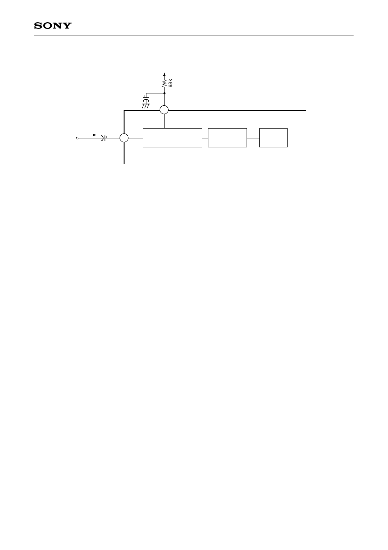
Fig. 1. Sync discrimination circuit block diagram
Fig. 1 shows the block diagram for the sync discrimination circuit. The signal input from Pin 23 (CV1) is sync tip
clamped by the external element attached to Pin 22. This signal is compared with a threshold voltage which is
larger than the sync tip level. If the signal is smaller than the threshold level, it does not proceed to the
following stage. At this time, the IC determines that sync does not exist. If the signal is larger than the threshold
level, it proceeds to the duty discrimination block. If the duty is greater than 91%, the duty discrimination block
determines that sync exists and sends the data to the I2C. If the duty is less than 84%, sync is determined not
to exist and the data is sent to the I2C. The duty discrimination block also has a time constant. After sync is
determined to exist, the sync status is held for approximately 14H (NTSC signal) even if the IC goes to a status
where sync does not exist such as no signal, etc. If there is no signal or sync does not exist for longer than
14H, the status switches from sync exists to sync does not exist.
– 18 –
Share Link: 