UPD78F0512AGA-GAM-AX 데이터 시트보기 (PDF) - Renesas Electronics
부품명
상세내역
제조사
UPD78F0512AGA-GAM-AX Datasheet PDF : 982 Pages
| |||
78K0/Kx2
CHAPTER 1 OUTLINE
1.1.3 Time Instruction cycle, peripheral hardware clock frequency, external main system clock frequency,
external main system clock input high-level width, and external main system clock input low-level width
(AC characteristics)
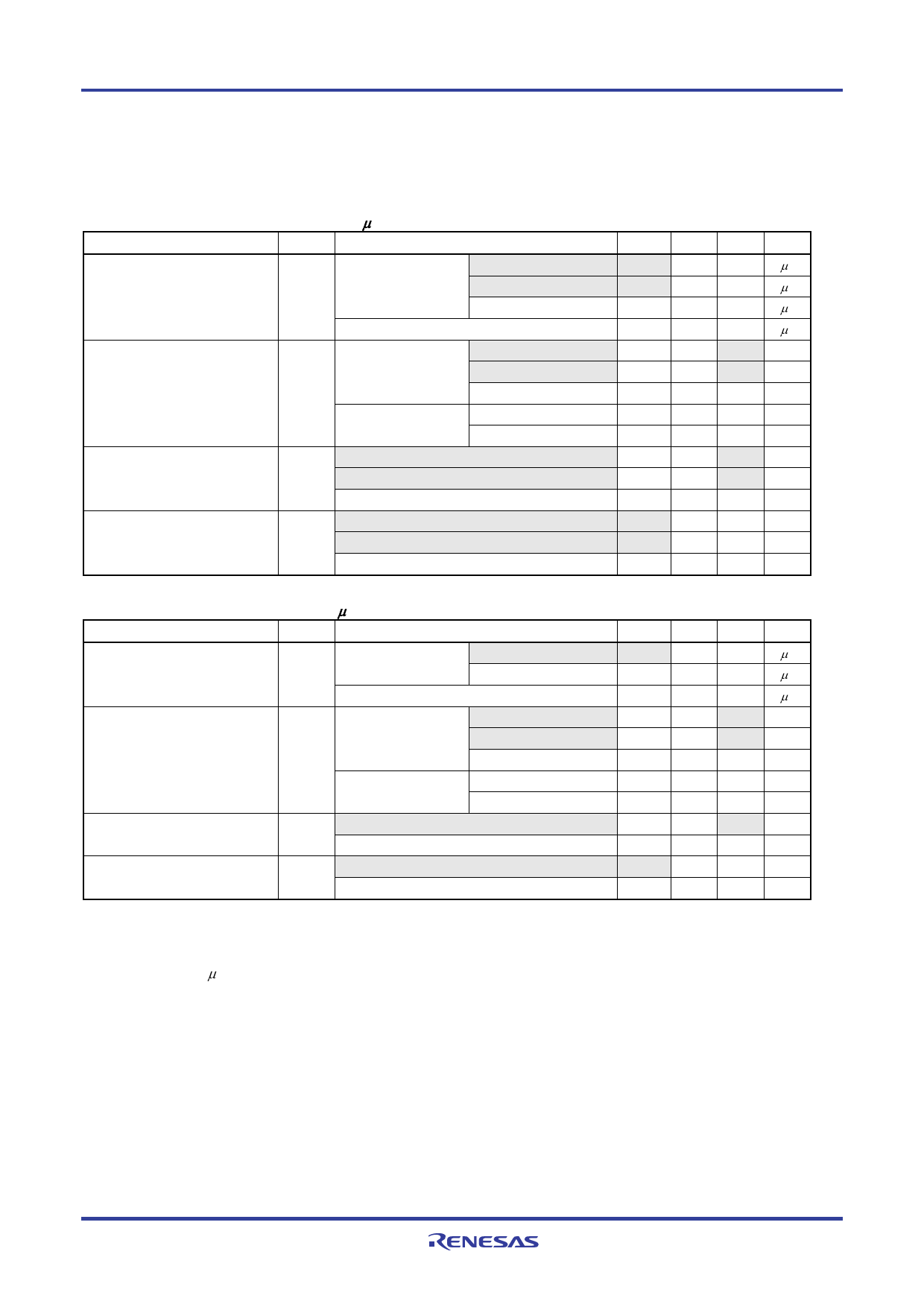
(1) Conventional-specification products (μPD78F05xx and 78F05xxD)
Parameter
Symbol
Conditions
MIN.
Instruction cycle (minimum
instruction execution time)
TCY
Main system clock (fXP) 4.0 V ≤ VDD ≤ 5.5 V
0.1
operation
2.7 V ≤ VDD < 4.0 V
0.2
1.8 V ≤ VDD < 2.7 V Note 1
0.4Note 3
Subsystem clock (fSUB) operationNote 2
114
Peripheral hardware clock
frequency
fPRS
fPRS = fXH
(XSEL = 1)
4.0 V ≤ VDD ≤ 5.5 V
2.7 V ≤ VDD < 4.0 V
1.8 V ≤ VDD < 2.7 V Note 1
External main system clock
frequency
fEXCLK
fPRS = fRH
(XSEL = 0)
2.7 V ≤ VDD ≤ 5.5 V
1.8 V ≤ VDD < 2.7 V Notes 1, 5
4.0 V ≤ VDD ≤ 5.5 V
2.7 V ≤ VDD < 4.0 V
1.8 V ≤ VDD < 2.7 V Note 1
7.6
7.6
1.0Note 6
1.0Note 6
1.0
External main system clock input tEXCLKH, 4.0 V ≤ VDD ≤ 5.5 V
24
high-level width, low-level width tEXCLKL 2.7 V ≤ VDD < 4.0 V
48
1.8 V ≤ VDD < 2.7 V Note 1
96
TYP.
122
MAX.
32
32
32
125
20
10
5
8.4
10.4
20.0
10.0
5.0
Unit
μs
μs
μs
μs
MHz
MHz
MHz
MHz
MHz
MHz
MHz
MHz
ns
ns
ns
(2) Expanded-specification products (μPD78F05xxA and 78F05xxDA)
Parameter
Symbol
Conditions
MIN.
Instruction cycle (minimum
instruction execution time)
TCY
Main system clock (fXP) 2.7 V ≤ VDD ≤ 5.5 V
0.1
operation
1.8 V ≤ VDD < 2.7 V Note 1
0.4Note 3
Subsystem clock (fSUB) operationNote 2
114
Peripheral hardware clock
frequency
fPRS
fPRS = fXH
(XSEL = 1)
4.0 V ≤ VDD ≤ 5.5 V
2.7 V ≤ VDD < 4.0 V Note 4
1.8 V ≤ VDD < 2.7 V Note 1
External main system clock
frequency
fEXCLK
fPRS = fRH
(XSEL = 0)
2.7 V ≤ VDD ≤ 5.5 V
1.8 V ≤ VDD < 2.7 V Notes 1, 5
2.7 V ≤ VDD ≤ 5.5 V
1.8 V ≤ VDD < 2.7 V Note 1
7.6
7.6
1.0Note 6
1.0
External main system clock input tEXCLKH, 2.7 V ≤ VDD ≤ 5.5 V
24
high-level width, low-level width tEXCLKL 1.8 V ≤ VDD < 2.7 V Note 1
96
TYP.
122
MAX.
32
32
125
20
20
5
8.4
10.4
20.0
5.0
Unit
μs
μs
μs
MHz
MHz
MHz
MHz
MHz
MHz
MHz
ns
ns
Notes 1.
2.
3.
4.
5.
6.
Standard and (A) grade products only
The 78K0/KB2 is not provided with a subsystem clock.
0.38 μs when operating with the 8 MHz internal oscillator.
Characteristics of the main system clock frequency. Set the division clock to be set by a peripheral function
to fXH/2 (10 MHz) or less. The multiplier/divider, however, can operate on fXH (20 MHz).
Characteristics of the main system clock frequency. Set the division clock to be set by a peripheral function
to fRH/2 or less.
2.0 MHz (MIN.) when using UART6 during on-board programming.
R01UH0008EJ0401 Rev.4.01
21
Jul 15, 2010
Share Link: 