MT8843 데이터 시트보기 (PDF) - Zarlink Semiconductor Inc
부품명
상세내역
제조사
MT8843 Datasheet PDF : 23 Pages
| |||
MT8843
burst. The U.K.’s CCA specifies that data can be
transmitted in either format.
Bellcore specification GR-30-CORE specifies
generic requirements for transmitting asynchronous
voiceband data to Customer Premises Equipment
(CPE). Another Bellcore specification SR-TSV-
002476 describes the same requirements from the
CPE’s perspective. The data transmission technique
specified in both documents is applicable in a variety
of services like Calling Number Delivery (CND),
Calling Name Delivery (CNAM) and Calling Identity
Delivery on Call Waiting (CIDCW) - services
promoted by Bellcore.
In CND/CNAM service, information about a calling
party is embedded in the silent interval between the
first and second ring burst. CNIC2 detects the first
ring burst and can then be setup to receive and
demodulate the incoming Bell-202 FSK data. The
device will output the demodulated data onto a 3-
wire serial interface.
In CIDCW service, information about an incoming
caller is sent to the subscriber, while they are
engaged in another call. A CPE Alerting Signal
(CAS) indicates the arrival of CIDCW information.
CNIC2 can detect the alert signal and then be setup
to demodulate incoming FSK data containing
CIDCW information.
Functional Description
Detection of CLIP/CID Call Arrival Indicators
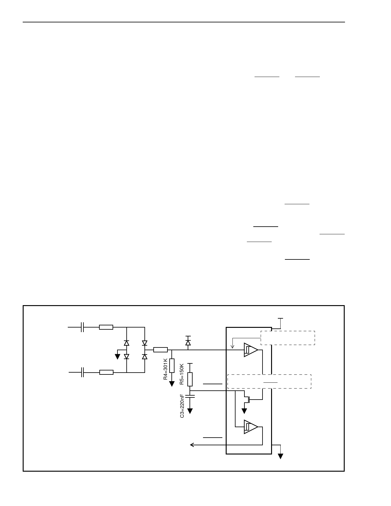
The circuit in Figure 3 illustrates the relationship
between the TRIGin, TRIGRC and TRIGout signals.
Typically, the three pin combination is used to detect
an event indicated by an increase of the TRIGin
voltage from VSS to above the Schmitt trigger high
going threshold VT+ (see DC electrical
characteristics).
Figure 3 shows a circuit to detect any one of three
CLIP/CID call arrival indicators: line reversal, ring
burst and ringing.
1. Line Reversal Detection
Line reversal, or polarity reversal on the A and B
wires indicates the arrival of an incoming CDS call,
as specified in SIN227. When the event (line
reversal) occurs, TRIGin rises past the high going
Schmitt threshold VT+ and TRIGout, which is
normally high, is pulled low. When the event is over,
TRIGin falls back to below the low going Schmitt
threshold VT- and TRIGout returns high. The
components R5 and C3 (see figure 3) at TRIGRC
ensure a minimum TRIGout low interval.
In a TE designed for CLIP, the TRIGout high to low
transition may be used to interrupt or wake-up the
microcontroller. The controller can thus be put into
C1=100nF
Tip/A
V1
V3
R1=499K
R3=200K
TRIGin
4.5V<VDD< 5.5V
MT8843
max VT+ = 0.68 VDD
min VT+ = 0.48 VDD
C2=100nF
Ring/B
V2
R2=499K V4
Notes:
The application circuit must ensure that,
VTRIGin>max VT+
where max VT+=3.74V @VDD=5.5V.
Tolerance to noise between A/B and VSS is:
max Vnoise = (min VT+)/0.30+0.7 =5.6Vrms @4.5V VDD
where min VT+ = 2.16V @VDD=4.5V.
Suggested R5C3 component values:
R5 from 10KΩ to 500KΩ
C3 from 47nF to 0.68µF
An example is C3=220nF, R5=150KΩ; TRIGout low
from 21.6ms to 37.6ms after TRIGin Signal stops
triggering the circuit.
TRIGRC
To determine values for C3 and R5:
R5C3=-t / ln(1-VTRIGRC/VDD)
TRIGout
To Microcontroller
Figure 3 - Circuit to Detect Line Reversal, Ring Burst and Ringing
5-34
Share Link: 