AD9814 데이터 시트보기 (PDF) - Analog Devices
부품명
상세내역
제조사
AD9814 Datasheet PDF : 15 Pages
| |||
AD9814
PGA Gain Registers
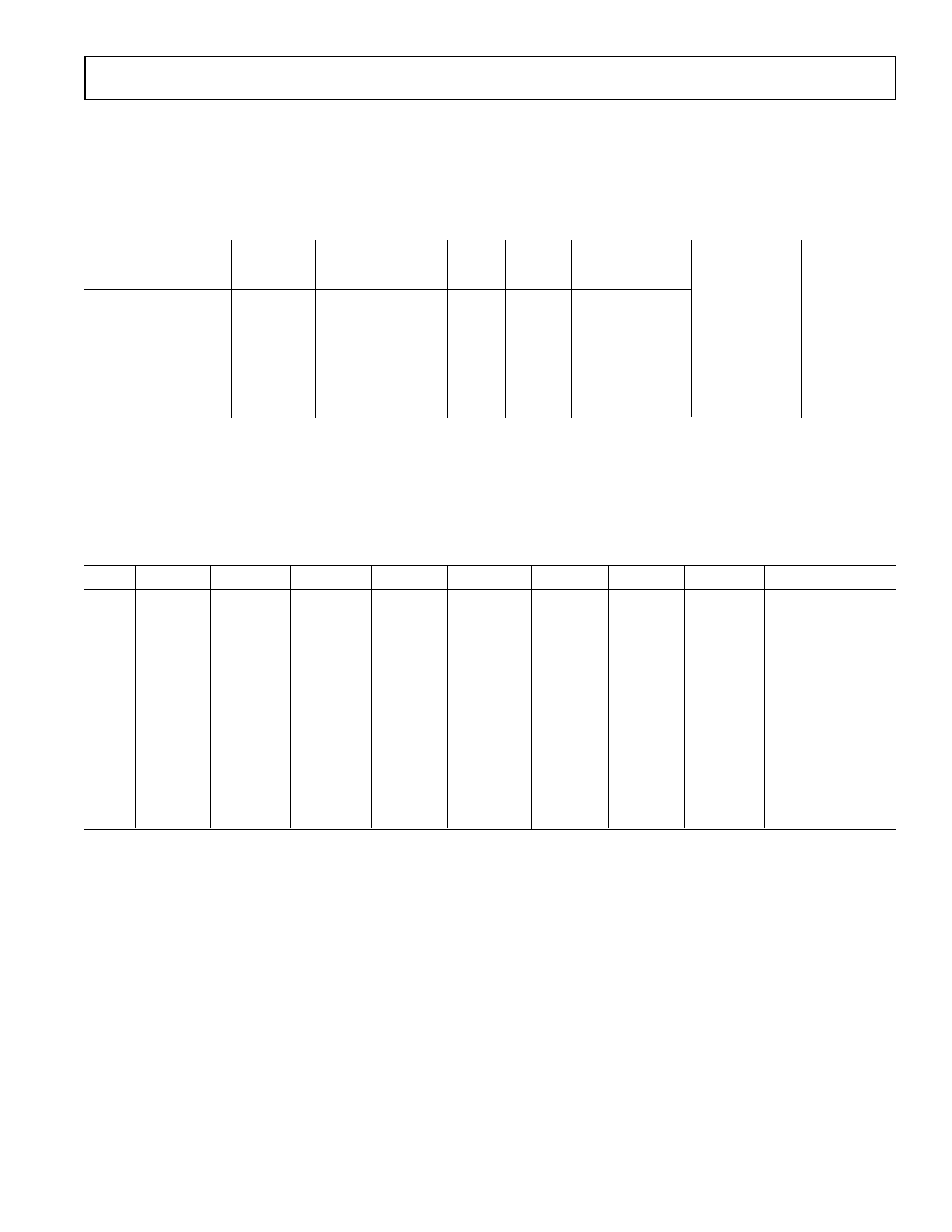
There are three PGA registers for individually programming the gain in the red, green and blue channels. Bits D8, D7 and D6 in
each register must be set low, and bits D5 through D0 control the gain range in 64 increments. See Figure 13 for a graph of the PGA
Gain versus PGA register code. The coding for the PGA registers is straight binary, with an all “zeros” word corresponding to the
minimum gain setting (1x) and an all “ones” word corresponding to the maximum gain setting (5.8x).
D8
Set to 0
0
0
D7
Set to 0
0
0
D6
Set to 0
0
0
0
0
0
0
0
0
*Power-on default value.
Table IV. PGA Gain Register Settings
D5
MSB
0
0
1
1
D4 D3
0
0
0
0
•
•
•
1
1
1
1
D2
D1 D0
LSB
0
0
0*
0
0
1
1
1
0
1
1
1
Gain (V/V) Gain (dB)
1.0
1.013
•
•
•
5.4
5.8
0.0
0.12
•
•
•
14.6
15.25
Offset Registers
There are three PGA registers for individually programming the offset in the red, green and blue channels. Bits D8 through D0 con-
trol the offset range from –300 mV to +300 mV in 512 increments. The coding for the offset registers is sign magnitude, with D8 as
the sign bit. Table V shows the offset range as a function of the Bits D8 through D0.
D8
D7
D6
MSB
0
0
0
0
0
0
0
1
1
1
0
0
1
0
0
1
1
1
*Power-on default value.
Table V. Offset Register Settings
D5
D4
D3
D2
D1
0
0
0
0
0
0
0
0
0
0
•
•
•
1
1
1
1
1
0
0
0
0
0
0
0
0
0
0
•
•
•
1
1
1
1
1
D0
Offset (mV)
LSB
0*
0
1
+1.2
•
•
•
1
+300
0
0
1
–1.2
•
•
•
1
–300
REV. 0
–11–
Share Link: 