HI-3583PCIF-10_06 데이터 시트보기 (PDF) - Holt Integrated Circuits
부품명
상세내역
제조사
HI-3583PCIF-10_06 Datasheet PDF : 16 Pages
| |||
HI-3582, HI-3583
FUNCTIONAL DESCRIPTION (cont.)
Once a valid ARINC word is loaded into the FIFO, then EOS
clocks the data ready flag flip flop to a "1", D/R1 or D/R2 (or both)
will go low. The data flag for a receiver will remain low until both
ARINC bytes from that receiver are retrieved and the FIFO is
empty. This is accomplished by first activating EN with SEL, the
byte selector, low to retrieve the first byte and then activating EN
with SEL high to retrieve the second byte. EN1 retrieves data
from receiver 1 and EN2 retrieves data from receiver 2.
Up to 32 ARINC words may be loaded into each receiver’s FIFO.
The FF1 (FF2) pin will go low when the receiver 1 (2) FIFO is full.
Failure to retrieve data from a full FIFO will cause the next valid
ARINC word received to overwrite the existing data in FIFO
location 32. A FIFO half full flag HF1 (HF2) goes low if the FIFO
contains 16 or more received ARINC words. The HF1 (HF2) pin is
intended to act as an interrupt flag to the system’s external
microprocessor, allowing a 16 word data retrieval routine to be
performed, without the user needing to continually poll the
HI-8582/HI-8583 status register bits.
LABEL RECOGNITION
The chip compares the incoming label to the stored labels if label
recognition is enabled. If a match is found, the data is processed.
If a match is not found, no indicators of receiving ARINC data are
presented. Note that 00(Hex) is treated in the same way as any
other label value. Label bit significance is not changed by the
status of control register bit CR15. Label bits BD00 - BD07 are
always compared to received ARINC bits 1 - 8 respectively.
LOADING LABELS
After a write that takes CR1 from 0 to 1, the next 16 writes of data
(PL pulsed low) load label data into each location of the label
memory from the BD00 - BD07 pins. The PL1 pin is used to write
label data for receiver 1 and PL2 for receiver 2. Note that ARINC
word reception is suspended during the label memory write
sequence.
READING LABELS
After the write that changes CR1 from 0 to 1, the next 16 data
reads of the selected receiver (EN taken low) are labels. EN1 is
used to read labels for receiver 1, and EN2 to read labels for
receiver 2. Label data is presented on BD0-BD7.
When writing to, or reading from the label memory, SEL must be a
one, all 16 locations should be accessed, and CR1 must be
written to zero before returning to normal operation. Label
recognition must be disabled (CR2/3=0) during the label read
sequence.
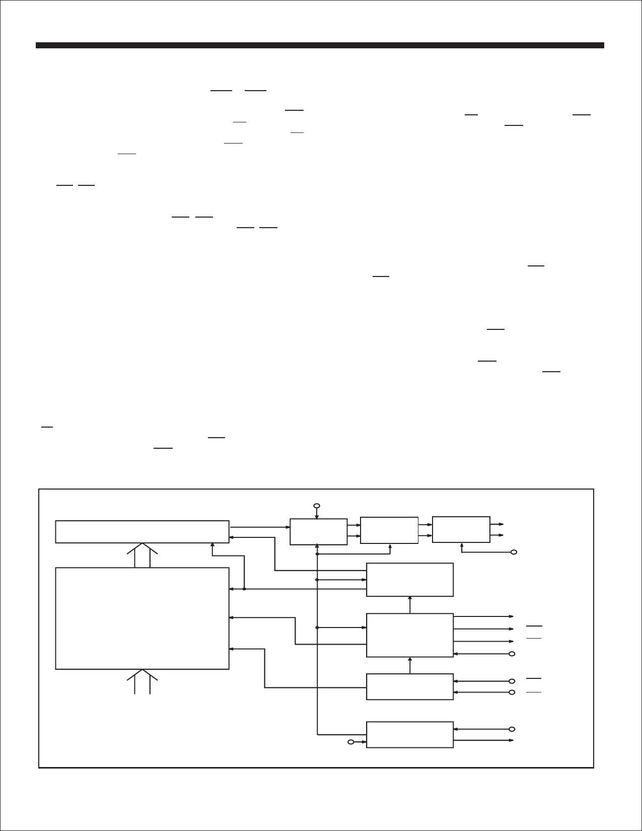
TRANSMITTER
FIFO OPERATION
The FIFO is loaded sequentially by first pulsing PL1 to load byte 1
and then PL2 to load byte 2. The control logic automatically loads
the 31 bit word (or 32 bit word if CR4=0) in the next available
position of the FIFO. If TX/R, the transmitter ready flag is high
(FIFO empty), then up to 32 words, each 31 or 32 bits long, may
be loaded. If TX/R is low, then only the available positions may be
loaded. If all 32 positions are full, the FFT flag is asserted and the
FIFO ignores further attempts to load data.
A transmitter FIFO half-full flag HFT is provided. When the
transmit FIFO contains less than 16 words, HFT is high,
indicating to the system microprocessor that a 16 ARINC word
block write sequence can be initiated.
In normal operation (CR4=1), the 32nd bit transmitted is a parity
bit. Odd or even parity is selected by programming control
register bit CR12 to a zero or one. If CR4 is programmed to a 0,
then all 32-bits of data loaded into the transmitter FIFO are treated
as data and are transmitted.
CR4,12
32 BIT PARALLEL
LOAD SHIFT REGISTER
32 x 32 FIFO
DATA BUS
BIT CLOCK
PARITY
GENERATOR
WORD CLOCK
ADDRESS
LOAD
DATA AND
NULL TIMER
SEQUENCER
LINE DRIVER
BIT
AND
WORD GAP
COUNTER
START
SEQUENCE
WORD COUNTER
AND
FIFO CONTROL
INCREMENT
WORD COUNT
FIFO
LOADING
SEQUENCER
TXAOUT
TXBOUT
TEST
TX/R
HFT
FFT
ENTX
PL1
PL2
DATA
CLOCK
CR13
DATA CLOCK
DIVIDER
FIGURE 3. TRANSMITTER BLOCK DIAGRAM
CLK
TX CLK
HOLT INTEGRATED CIRCUITS
6
Share Link: 