LC66354C 데이터 시트보기 (PDF) - SANYO -> Panasonic
부품명
상세내역
제조사
LC66354C Datasheet PDF : 21 Pages
| |||
LC66354C, 66356C, 66358C
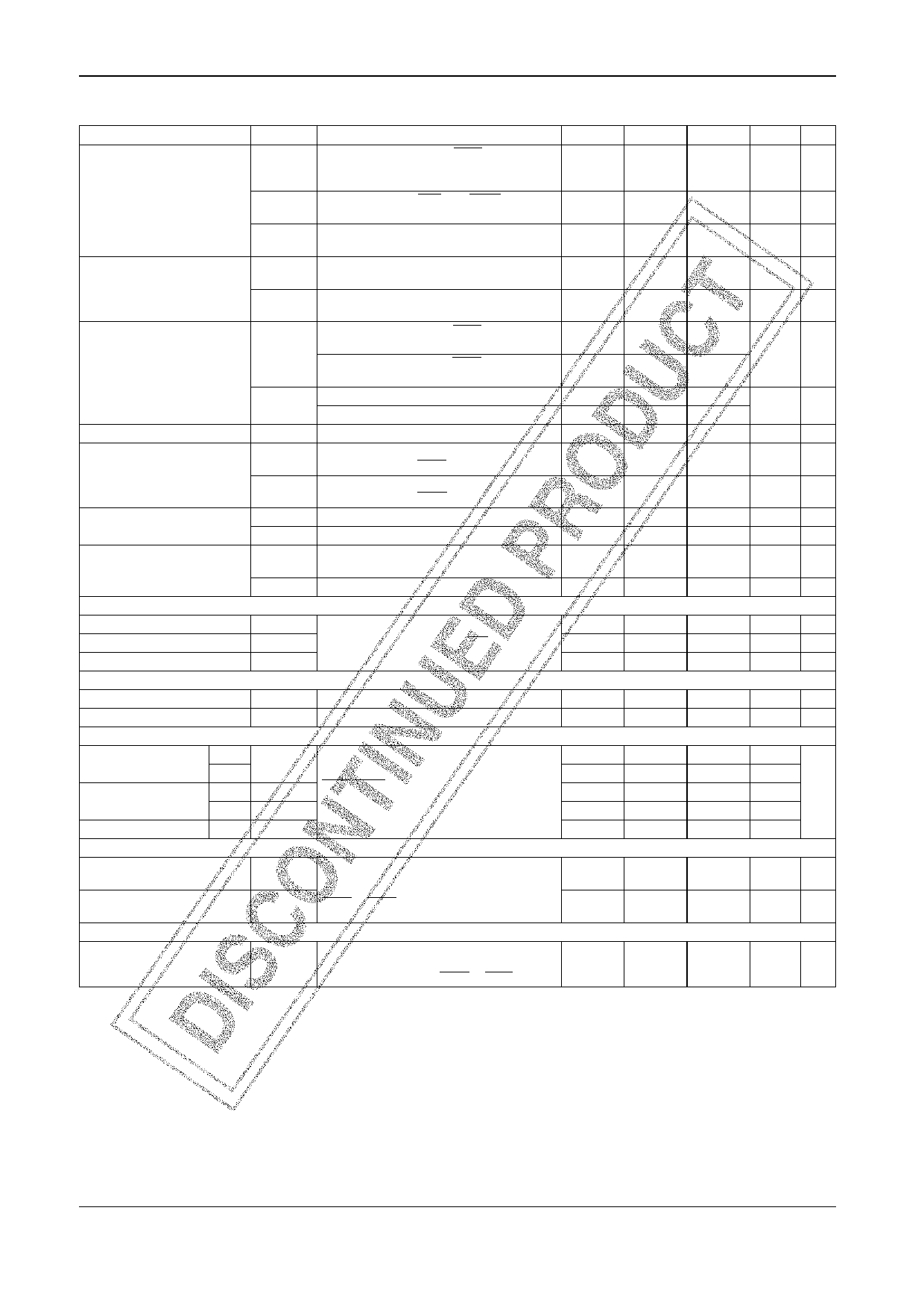
Electrical Characteristics at Ta = –30 to +70°C, VSS = 0 V, VDD = 2.5 to 5.5 V unless otherwise specified.
Parameter
Input high-level current
Input low-level current
Output high-level voltage
Output pull-up current
Output low-level voltage
Output off leakage current
Comparator offset voltage
[Schmitt characteristics]
Hysteresis voltage
High-level threshold voltage
Low-level threshold voltage
[Ceramic oscillator]
Oscillator frequency
Oscillator stabilization time
[Serial clock]
Cycle time
Input
Output
Low-level and high-level Input
pulse widths
Output
Rise an fall times
Output
[Serial input]
Symbol
IIH1
IIH2
IIH3
IIL1
IIL2
VOH1
VOH2
IPO
VOL1
VOL2
IOFF1
IOFF2
VOFF1
VOFF2
VHIS
Vt H
Vt L
fCF
fCFS
tCKCY
tCKL
tCKH
tCKR, tCKF
Conditions
P2, P3 (except for the P33/HOLD pin),
P4, P5, and P6: VIN = 13.5 V, with the output
Nch transistor off
P0, P1, PC, OSC1, RES, P33/HOLD:
VIN = VDD, with the output Nch transistor off
PD, PE, PC2, PC3: VIN = VDD,
with the output Nch transistor off
Input ports other than PD, PE, PC2, and PC3:
VIN = VSS, with the output Nch transistor off
PC2, PC3, PD, PE: VIN = VSS,
with the output Nch transistor off
P2, P3 (except for the P33/HOLD pin),
P6, and PC: IOH = –1 mA
P2, P3 (except for the P33/HOLD pin),
P6, and PC: IOH = –0.1 mA
P0, P1, P4, P5: IOH = –50 µA
P0, P1, P4, P5: IOH = –30 µA
P0, P1, P4, P5: VIN = VSS, VDD = 5.5 V
P0, P1, P2, P3, P4, P5, P6, and PC
(except for the P33/HOLD pin): IOL = 1.6 mA
P0, P1, P2, P3, P4, P5, P6, and PC
(except for the P33/HOLD pin): IOL = 8 mA
P2, P3, P4, P5, P6: VIN = 13.5 V
P0, P1, PC: VIN = VDD
PD1 to PD3: VIN = VSS to VDD – 1.5 V,
VDD = 3.0 to 5.5 V
PD0: VIN = 1.5 to VDD, VDD = 3.0 to 5.5 V
P2, P3, P5, P6, OSC1 (EXT), RES
OSC1, OSC2: Figure 2, 4 MHz
Figure 3, 4 MHz
SCK0, SCK1: With the timing of Figure 4 and
the test load of Figure 5.
min
–1.0
–1.0
VDD – 1.0
VDD – 0.5
VDD – 1.0
VDD – 0.5
–1.6
0.5 VDD
0.2 VDD
0.9
2.0
0.4
1.0
Data setup time
Data hold time
[Serial output]
Output delay time
tICK
SI0, SI1: With the timing of Figure 4.
0.3
Stipulated with respect to the rising edge (↑) of
tCKI
SCK0 or SCK1.
0.3
tCKO
SO0, SO1: With the timing of Figure 4 and
the test load of Figure 5. Stipulated with respect
to the falling edge (↓) of SCK0 or SCK1.
typ
±50
±50
0.1 VDD
4.0
max
5.0
1.0
1.0
0.4
1.5
5.0
1.0
±300
±300
0.8 VDD
0.5 VDD
10
0.1
0.3
Unit Note
µA
1
µA
1
µA
1
µA
2
µA
2
V
3
V
4
mA
4
V
5
V
µA
5
µA
5
mV
mV
V
V
MHz
ms
µs
Tcyc
µs
Tcyc
µs
µs
µs
Continued on next page.
No. 5484-10/21
Share Link: 