LC66354C 데이터 시트보기 (PDF) - SANYO -> Panasonic
부품명
상세내역
제조사
LC66354C Datasheet PDF : 21 Pages
| |||
LC66354C, 66356C, 66358C
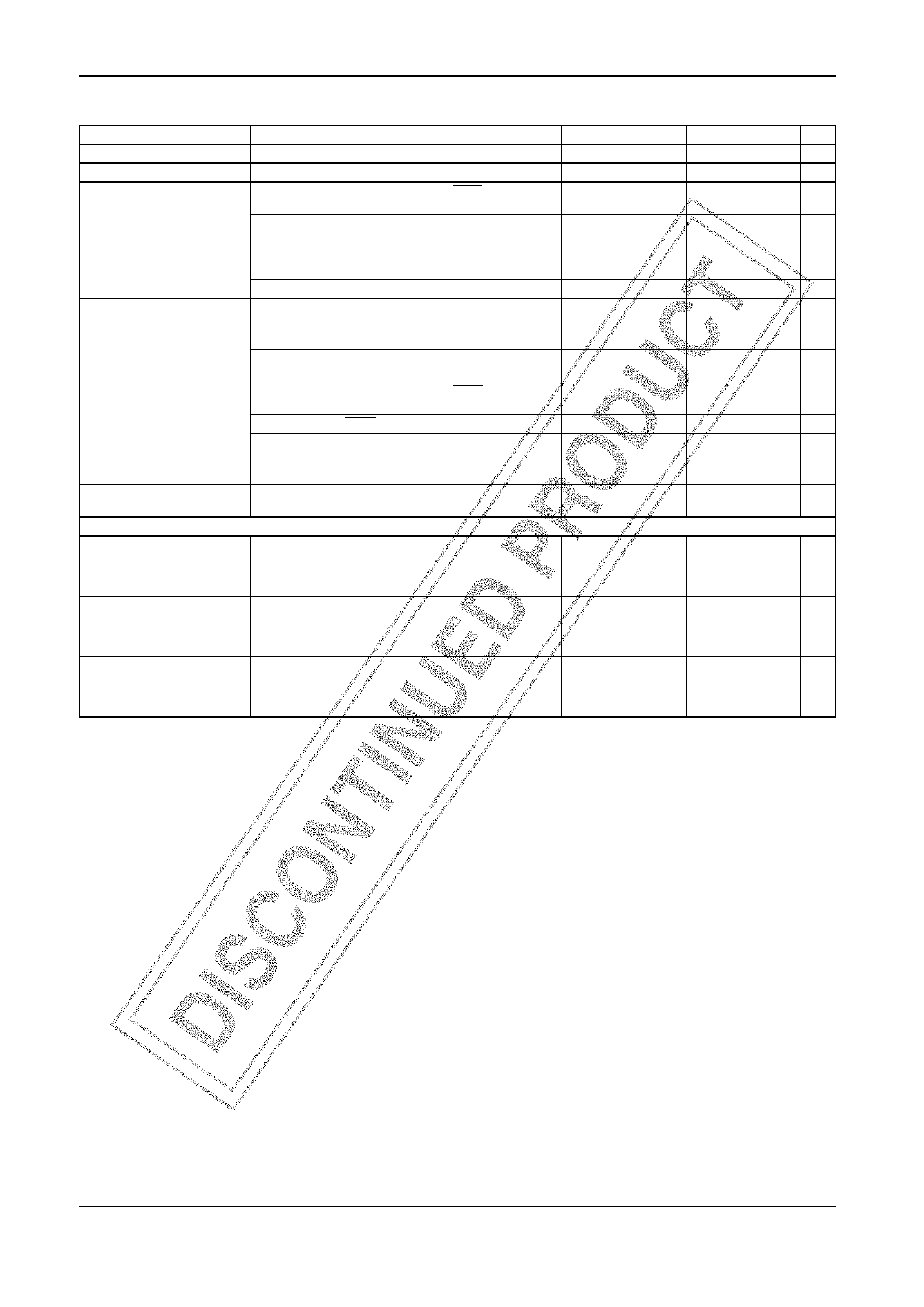
Allowable Operating Ranges at Ta = –30 to +70°C, VSS = 0 V, VDD = 2.5 to 5.5 V, unless otherwise specified.
Parameter
Symbol
Conditions
min
typ
max
Unit Note
Operating supply voltage
Memory retention supply voltage
VDD
VDDH
VIH1
VDD: 0.92 Tcyc 10 µs
VDD: During hold mode
P2, P3 (except for the P33/HOLD pin), P4, P5,
and P6: N-channel output transistor off
2.5
1.8
0.8 VDD
5.5 V
5.5 V
+13.5 V
1
Input high-level voltage
VIH2
VIH3
P33/HOLD, RES, OSC1:
N-channel output transistor off
P0, P1, PC, PD, PE:
N-channel output transistor off
0.8 VDD
0.8 VDD
VDD
V
2
VDD
V
3
Mid-level input voltage
Common-mode input
voltage range
VIH4
VIM
VCMM1
VCMM2
VIL1
PE: With 3-value input used, VDD = 3.0 to 5.5 V
PE: With 3-value input used, VDD = 3.0 to 5.5 V
PD0, PC2: When the comparator input is used,
VDD = 3.0 to 5.5 V
PD1, PD2, PD3, PC3: When the comparator
input is used, VDD = 3.0 to 5.5 V
P2, P3 (except for the P33/HOLD pin), P5, P6,
RES, and OSC1: N-channel output transistor off
0.8 VDD
0.4 VDD
1.5
VSS
VDD
V
0.6 VDD
V
VDD
V
VDD – 1.5
V
0.2 VDD
V
2
Input low-level voltage
VIL2
P33/HOLD: VDD = 1.8 to 5.5 V
P0, P1, P4, PC, PD, PE, TEST:
VIL3
N-channel output transistor off
0.2 VDD
V
VSS
0.2 VDD
V
3
Operating frequency
(instruction cycle time)
VIL4
PE: With 3-value input used, VDD = 3.0 to 5.5 V
VSS
fop
0.4
(Tcyc)
(10)
0.2 VDD
4.35
(0.92)
V
MHz
(µs)
[External clock input conditions]
Frequency
OSC1: Defined by Figure 1. Input the clock
signal to OSC1 and leave OSC2 open.
fext
(External clock input must be selected as the
0.4
oscillator circuit option.)
4.35 MHz
OSC1: Defined by Figure 1. Input the clock
signal to OSC1 and leave OSC2 open.
Pulse width
textH, textL (External clock input must be selected as the
100
ns
oscillator circuit option.)
Rise and fall times
textR, textF
OSC1: Defined by Figure 1. Input the clock
signal to OSC1 and leave OSC2 open.
(External clock input must be selected as the
oscillator circuit option.)
30 ns
Note: 1. Applies to pins with open-drain specifications. However, VIH2 applies to the P33/HOLD pin.
When ports P2, P3, and P6 have CMOS output specifications they cannot be used as input pins.
2. Applies to pins with open-drain specifications.
3. When RE is used as a three-value input, VIH4, VIM, and VIL4 apply. When the ports PC pins have CMOS output specifications they cannot be used
as input pins.
No. 5484-9/21
Share Link: 