CXD1961AQ 데이터 시트보기 (PDF) - Sony Semiconductor
부품명
상세내역
제조사
CXD1961AQ Datasheet PDF : 33 Pages
| |||
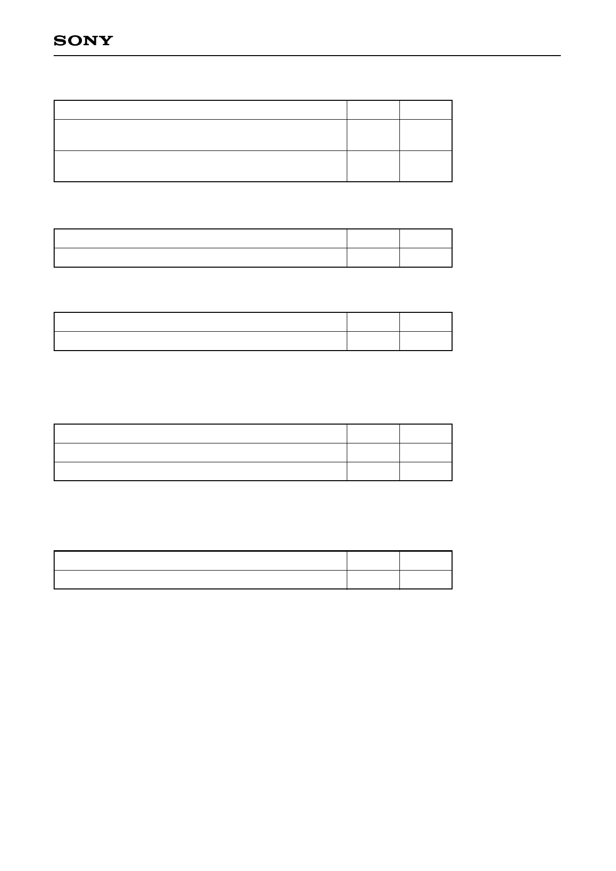
2-3. Clock Recovery
Function
Clock error output
(for clock recovery by VCXO)
Recovered symbol clock output
(switchable to sampling clock output)
3. Carrier Recovery
Function
Carrier lock flag (H: lock)
4. AGC
Function
AGC control data (PWM output)
See reference circuit (4)
Pin No. Pin name
70 to 73 CR0 to 3
76 to 79 CR4 to 7
69
CKV
Pin No. Pin name
82
QSYNC
Pin No. Pin name
68 AGCPWM
5. Viterbi Decoder
Function
Viterbi clock output
Viterbi decoded data output
Pin No.
65
64
Pin name
VCK
VDT
These pins can be fixed to ground by setting CPU I/F register 0E (hex).
6. Frame Synchronization
Function
Frame synchronization flag (H: sync)
Pin No. Pin name
83
FSYNC
CXD1961AQ
– 11 –
Share Link: 