EL5111T 데이터 시트보기 (PDF) - Renesas Electronics
부품명
상세내역
제조사
EL5111T Datasheet PDF : 14 Pages
| |||
EL5111T
Absolute Maximum Ratings (TA = +25°C)
Supply Voltage between VS+ and VS- . . . . . . . . . . . .+19.8V
Input Voltage Range (VIN+, VIN-). . . VS- - 0.5V, VS+ + 0.5V
Input Differential Voltage (VIN+ - VIN-). . . . . . . . . . . . . . . .
. . . . . . . . . . . . . . . . . . . . . . . (VS+ + 0.5V)-(VS- - 0.5V)
Maximum Continuous Output Current . . . . . . . . . . . ±70mA
ESD Rating
Human Body Model . . . . . . . . . . . . . . . . . . . . . . . 3000V
Thermal Information
Thermal Resistance (Typical)
5 Ld TSOT (Notes 4, 5)
JA (°C/W) JC (°C/W)
215
290
Storage Temperature . . . . . . . . . . . . . . . . -65°C to +150°C
Ambient Operating Temperature . . . . . . . . . -40°C to +85°C
Maximum Junction Temperature . . . . . . . . . . . . . . . +150°C
Power Dissipation . . . . . . . . . . . . . . . See Figures 32 and 33
Pb-Free Reflow Profile . . . . . . . . . . . . . . . . . .see link below
http://www.intersil.com/pbfree/Pb-FreeReflow.asp
CAUTION: Do not operate at or near the maximum ratings listed for extended periods of time. Exposure to such conditions may adversely impact
product reliability and result in failures not covered by warranty.
NOTES:
4. JA is measured in free air with the component mounted on a high effective thermal conductivity test board. See Tech Brief
TB379.
5. For JC, the “case temp” location is taken at the package top center.
IMPORTANT NOTE: All parameters having Min/Max specifications are guaranteed. Typ values are for information purposes only. Unless otherwise noted, all tests are
at the specified temperature and are pulsed tests, therefore: TJ = TC = TA
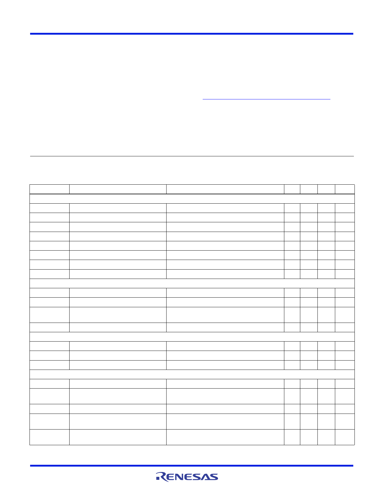
Electrical Specifications VS+ = +5V, VS- = -5V, RL = 1k to 0V, TA = +25°C, Unless Otherwise Specified.
PARAMETER
DESCRIPTION
CONDITIONS
MIN TYP MAX UNIT
INPUT CHARACTERISTICS
VOS
TCVOS
IB
RIN
CIN
CMIR
Input Offset Voltage
VCM = 0V
Average Offset Voltage Drift (Note 6)
Input Bias Current
Input Impedance
VCM = 0V
Input Capacitance
Common-Mode Input Range
5
18 mV
8
µV/°C
2
60
nA
1
G
2
pF
-5.5
+5.5 V
CMRR
Common-Mode Rejection Ratio
AVOL
Open-Loop Gain
OUTPUT CHARACTERISTICS
For VIN from -5.5V to 5.5V
-4.5V VOUT 4.5V
50 73
dB
62 78
dB
VOL
VOH
ISC
Output Swing Low
Output Swing High
Short-Circuit Current
IOUT
Output Current
POWER SUPPLY PERFORMANCE
IL = -5mA
IL = +5mA
VCM = 0V, Source: VOUTx short to VS-,
Sink: VOUT short to VS+
-4.93 -4.85 V
4.85 4.93
V
±300
mA
±70
mA
(VS+) - (VS-)
IS
PSRR
Supply Voltage Range
Supply Current
Power Supply Rejection Ratio
VCM = 0V, No load
Supply is moved from ±2.25V to ±9.5V
4.5
19
V
3.1 4
mA
60 75
dB
DYNAMIC PERFORMANCE
SR
tS
BW
GBWP
PM
Slew Rate (Note 7)
Settling to +0.1% (Note 8)
-3dB Bandwidth
Gain-Bandwidth Product
Phase Margin
-4.0V VOUT 4.0V, 20% to 80%
AV = +1, VOUTx= 2V step,
RL = 1k1k (probe), CL = 1.5pF
RL = 1kCL = 1.5pF
AV = -10, RF = 1kRG = 100
RL = 1k1k (probe), CL = 1.5pF
AV = -10, RF = 1kRG = 100
RL = 1k1k (probe), CL = 1.5pF
100
V/µs
85
ns
60
MHz
32
MHz
50
°
FN6894 Rev 0.00
May 27, 2010
Page 3 of 14
Share Link: 