ADSP-BF538 데이터 시트보기 (PDF) - Analog Devices
부품명
상세내역
제조사
ADSP-BF538 Datasheet PDF : 56 Pages
| |||
ADSP-BF538/ADSP-BF538F
The PC133-compliant SDRAM controller can be programmed
to interface to up to 128 Mbytes of SDRAM. The SDRAM con-
troller allows one row to be open for each internal SDRAM
bank, for up to four internal SDRAM banks, improving overall
system performance.
The asynchronous memory controller can be programmed to
control up to four banks of devices with very flexible timing
parameters for a wide variety of devices. Each bank occupies a
1 Mbyte segment regardless of the size of the devices used, so
that these banks will only be contiguous if each is fully popu-
lated with 1 Mbyte of memory.
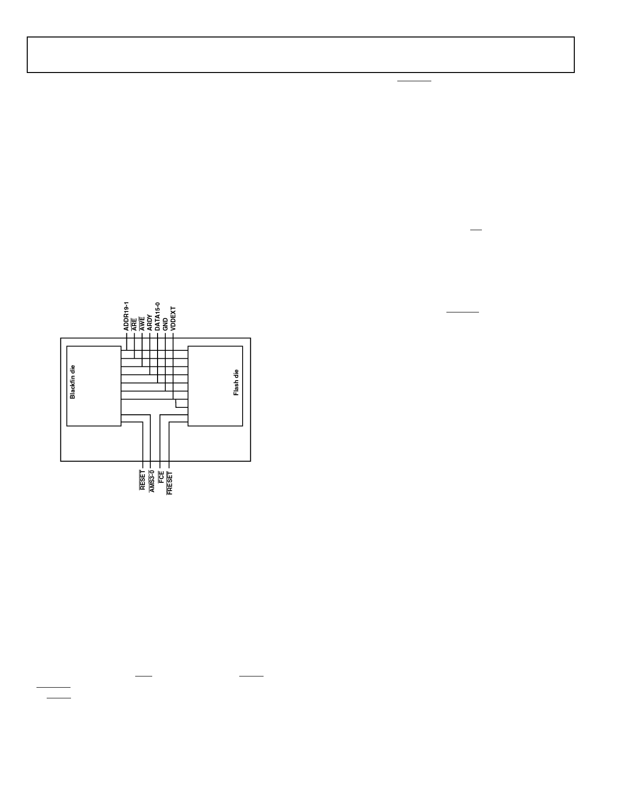
Flash Memory
The ADSP-BF538F4 and ADSP-BF538F8 processors contain a
separate flash die, connected to the EBIU bus, within the pack-
age of the processors. Figure 4 on Page 6 shows how the flash
memory die and Blackfin processor die are connected.
ADDR19-1
ARE
AWE
ARDY
DATA15-0
GND
VDDEXT
AMS3-0
RESET
ADSP-BF538Fx
package
A18-0
OE
WE
RY/BY
DQ15-0
VSS
VCC
BYTE
CE
RESET
Figure 4. Internal Connection of Flash Memory (ADSP-BF538Fx)
The ADSP-BF538F4 contains a 512 Kbits bottom boot sector
flash memory. The ADSP-BF538F8 contains a 1 Mbit bottom
boot sector flash memory. Features include the following.
• access times as fast as 70 ns (EBIU registers must be set
appropriately)
• sector protection
• one million write cycles per sector
• 20 year data retention
The Blackfin processor connects to the flash memory die with
address, data, chip enable, write enable, and output enable con-
trols as if it were an external memory device.
The flash chip enable pin FCE must be connected to AMS0 or
AMS3–1 through a printed circuit board trace. When connected
to AMS0 the Blackfin processor can boot from the flash die.
Preliminary Technical Data
When connected to AMS3–1 the flash memory will appear as
non-volatile memory in the processor memory map shown in
Figure 3 on Page 5.
Flash Memory Programming
The ADSP-BF538F4 and ADSP-BF538F8 flash memory may be
programmed before or after mounting on the printed circuit
board.
To program the flash prior to mounting on the printed circuit
board, use a hardware programming tool that can provide the
data, address, and control stimuli to the flash die through the
external pins on the package. During this programming, VDDEXT
and GND must be provided to the package and the Blackfin
must be held in reset with bus request (BR) asserted and a
CLKIN provided.
The VisualDSP++® tools may be used to program the flash
memory after the device is mounted on a printed circuit board.
Flash Memory Sector Protection
To use the sector protection feature, a high voltage (+12 V nom-
inal) must be applied to the flash FRESET pin. Refer to the flash
datasheet for details.
I/O Memory Space
Blackfin processors do not define a separate I/O space. All
resources are mapped through the flat 32-bit address space. On-
chip I/O devices have their control registers mapped into mem-
ory mapped registers (MMRs) at addresses near the top of the
4 Gbyte address space. These are separated into two smaller
blocks, one which contains the control MMRs for all core func-
tions, and the other which contains the registers needed for
setup and control of the on-chip peripherals outside of the core.
The MMRs are accessible only in supervisor mode and appear
as reserved space to on-chip peripherals.
Booting
The ADSP-BF538/ADSP-BF538F processors contain a small
boot kernel, which configures the appropriate peripheral for
booting. If the processors are configured to boot from boot
ROM memory space, the processors start executing from the
on-chip boot ROM. For more information, see Booting Modes
on Page 15.
Event Handling
The event controller on the ADSP-BF538/ADSP-BF538F pro-
cessors handle all asynchronous and synchronous events to the
processors. The processor provides event handling that sup-
ports both nesting and prioritization. Nesting allows multiple
event service routines to be active simultaneously. Prioritization
ensures that servicing of a higher priority event takes prece-
dence over servicing of a lower priority event. The controller
provides support for five different types of events:
• Emulation – An emulation event causes the processor to
enter emulation mode, allowing command and control of
the processor via the JTAG interface.
• Reset – This event resets the processor.
Rev. PrD | Page 6 of 56 | May 2006
Share Link: 