A8425 데이터 시트보기 (PDF) - Allegro MicroSystems
부품명
상세내역
제조사
A8425
Allegro MicroSystems

A8425 Datasheet PDF : 16 Pages
| |||
A8425
High Current Photoflash Capacitor Charger
with IGBT Driver for Two Li+ Batteries
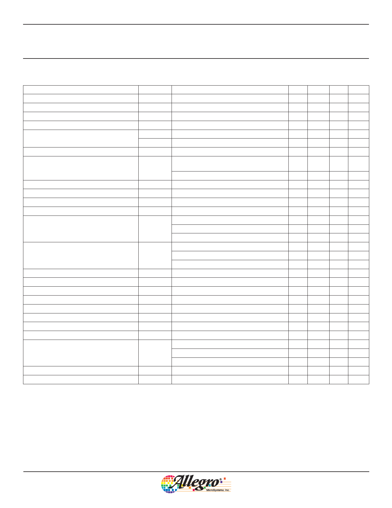
ELECTRICAL CHARACTERISTICS typical values valid at VIN = VBAT= 3.6 V, RSET = 40 kΩ, ISWlim = 2.0 A, and TA=25°C, unless otherwise noted
Characteristics
Symbol
Test Conditions
Min. Typ. Max. Unit
VBAT Pin Voltage Range1
VIN Pin Voltage Range1
UVLO Enable Threshold
UVLO Hysteresis
Switch Current Limit2
SW Current Limit to ISET Current Ratio
ISET Pin Voltage While Charging
ISET Pin Internal Resistance
GND Pin Internal Resistance
Switch On-Resistance
Switch Leakage Current1
VBAT
VIN
VINUV
VINUVhys
ISWlimMAX
ISWlimMIN
ISWlim/ISET
VSET
RSET(INT)
RGND(INT)
RSWDS(on)
ISWlk
VIN rising
Maximum, ISET = 55 μA
Minimum, ISET = 17 μA
ISET = 55 μA, CHARGE = high
ISET = 55 μA, CHARGE = high, ISW = 0 A (VBAT
disconnected)
ISET = 55 μA, CHARGE = high, ISW = 3.2 A
VIN = 3.6 V, ID = 800 mA, TA = 25°C
VSW = VBAT = 11 V, in shutdown
Shutdown (CHARGE = 0 V, TRIGGER = 0 V
1.5
–
11
V
3.0
–
5.5
V
2.55 2.65 2.75 V
–
150
–
mV
2.9
3.2
3.5
A
–
1.0
–
A
–
58.5
– kA/A
– 1.182 –
V
– 1.268 –
V
–
330
–
Ω
–
27
–
mΩ
–
0.2
–
Ω
–
–
1
μA
–
0.01
1
μA
VIN Pin Supply Current
IIN
Charging done
Charging (CHARGE = VIN, TRIGGER = 0 V)
Shutdown (CHARGE = 0 V, TRIGGER = 0 V)
–
25
50
μA
–
2
–
mA
–
0.01
1
μA
VBAT Pin Supply Current
CHARGE Pin Input Current
CHARGE Pin Input Voltage High1
CHARGE Pin Input Voltage Low1
CHARGE Pin Pull-down Resistor
Maximum Switch-off Timeout
Maximum Switch-on Timeout
¯D¯¯O¯¯N¯¯E¯ Pin Output Leakage Current1
¯D¯¯O¯¯N¯¯E¯ Pin Output Low Voltage1
Output Comparator Trip Voltage (measured as
VSW – VBAT; see 1 for VSEL= GND)
IBAT
ICHARGE
ICHARGE(H)
ICHARGE(L)
RCHARGE
toffMAX
tonMAX
IDONElk
VDONEL
VOUTTRIP
Charging done
Charging (CHARGE = VIN, TRIGGER = 0 V)
VCHARGE = VIN
Over input supply range, VIN
Over input supply range, VIN
32 μA into ¯D¯¯O¯¯N¯¯E¯ pin
VSEL = GND
VSEL = open
VSEL = VIN
–
–
1
μA
–
25
50
uA
–
36
–
μA
1.4
–
–
V
–
–
0.4
V
–
100
–
kΩ
–
18
–
μs
–
18
–
μs
–
–
1
μA
–
–
100 mV
31 31.5 32
V
–
35
–
V
–
39.4
–
V
Output Comparator Overdrive
Minimum dV/dt for ZVS Comparator
VOUTOV
dV/dt
200 ns pulse width (90% to 90%)
Measured at SW pin
–
200 400 mV
–
20
– V/μs
Continued on the next page …
Allegro MicroSystems, Inc.
5
115 Northeast Cutoff
Worcester, Massachusetts 01615-0036 U.S.A.
1.508.853.5000; www.allegromicro.com
Share Link: