MT48H16M16LFF-8 데이터 시트보기 (PDF) - Micron Technology
부품명
상세내역
제조사
MT48H16M16LFF-8 Datasheet PDF : 58 Pages
| |||
WRITEs
WRITE bursts are initiated with a WRITE command,
as shown in Figure 13.
The starting column and bank addresses are pro-
vided with the WRITE command, and auto precharge
is either enabled or disabled for that access. If auto
precharge is enabled, the row being accessed is
precharged at the completion of the burst. For the ge-
neric WRITE commands used in the following illustra-
tions, auto precharge is disabled.
During WRITE bursts, the first valid data-in ele-
ment will be registered coincident with the WRITE com-
mand. Subsequent data elements will be registered on
each successive positive clock edge. Upon completion
of a fixed-length burst, assuming no other commands
have been initiated, the DQs will remain High-Z and
any additional input data will be ignored (see Figure
14). A full-page burst will continue until terminated.
(At the end of the page, it will wrap to the start address
and continue.)
Data for any WRITE burst may be truncated with a
subsequent WRITE command, and data for a fixed-
length WRITE burst may be immediately followed by
data for a WRITE command. The new WRITE command
can be issued on any clock following the previous WRITE
command, and the data provided coincident with the
new command applies to the new command. An ex-
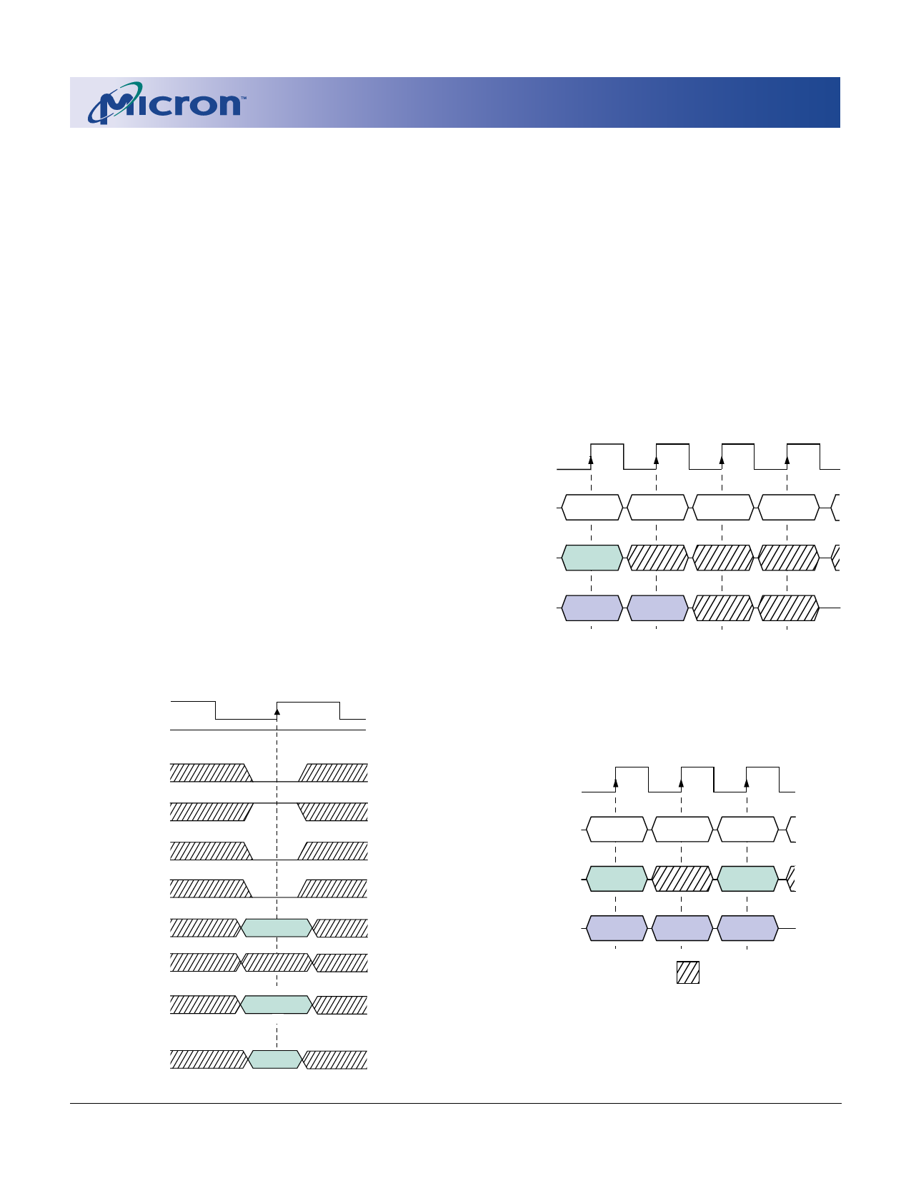
Figure 13
WRITE Command
CLK
CKE HIGH
CS#
RAS#
CAS#
WE#
A0-A8: x16
A9, A11: x16
A10
COLUMN
ADDRESS
ENABLE AUTO PRECHARGE
DISABLE AUTO PRECHARGE
BA0,1
BANK
ADDRESS
ADVANCE
256Mb: x16
MOBILE SDRAM
ample is shown in Figure 15. Data n + 1 is either the last
of a burst of two or the last desired of a longer burst. The
256Mb SDRAM uses a pipelined architecture and there-
fore does not require the 2n rule associated with a
prefetch architecture. A WRITE command can be initi-
ated on any clock cycle following a previous WRITE
command. Full-speed random write accesses within a
page can be performed to the same bank, as shown in
Figure 16, or each subsequent WRITE may be per-
formed to a different bank.
Figure 14
WRITE Burst
T0
T1
T2
T3
CLK
COMMAND
WRITE
NOP
NOP
NOP
ADDRESS
DQ
BANK,
COL n
DIN
n
DIN
n+1
Figure 15
WRITE to WRITE
T0
T1
T2
CLK
COMMAND
WRITE
NOP
WRITE
ADDRESS
BANK,
COL n
BANK,
COL b
DQ
DIN
n
DIN
n+1
DIN
b
DON’T CARE
NOTE: DQM is LOW. Each WRITE command may
be to any bank.
256Mb: x16 Mobile SDRAM
MobileRamY26L_A.p65 – Pub. 5/02
21
Micron Technology, Inc., reserves the right to change products or specifications without notice.
©2002, Micron Technology, Inc.
Share Link: 