EL5325 데이터 시트보기 (PDF) - Intersil
부품명
상세내역
제조사
EL5325 Datasheet PDF : 11 Pages
| |||
EL5325
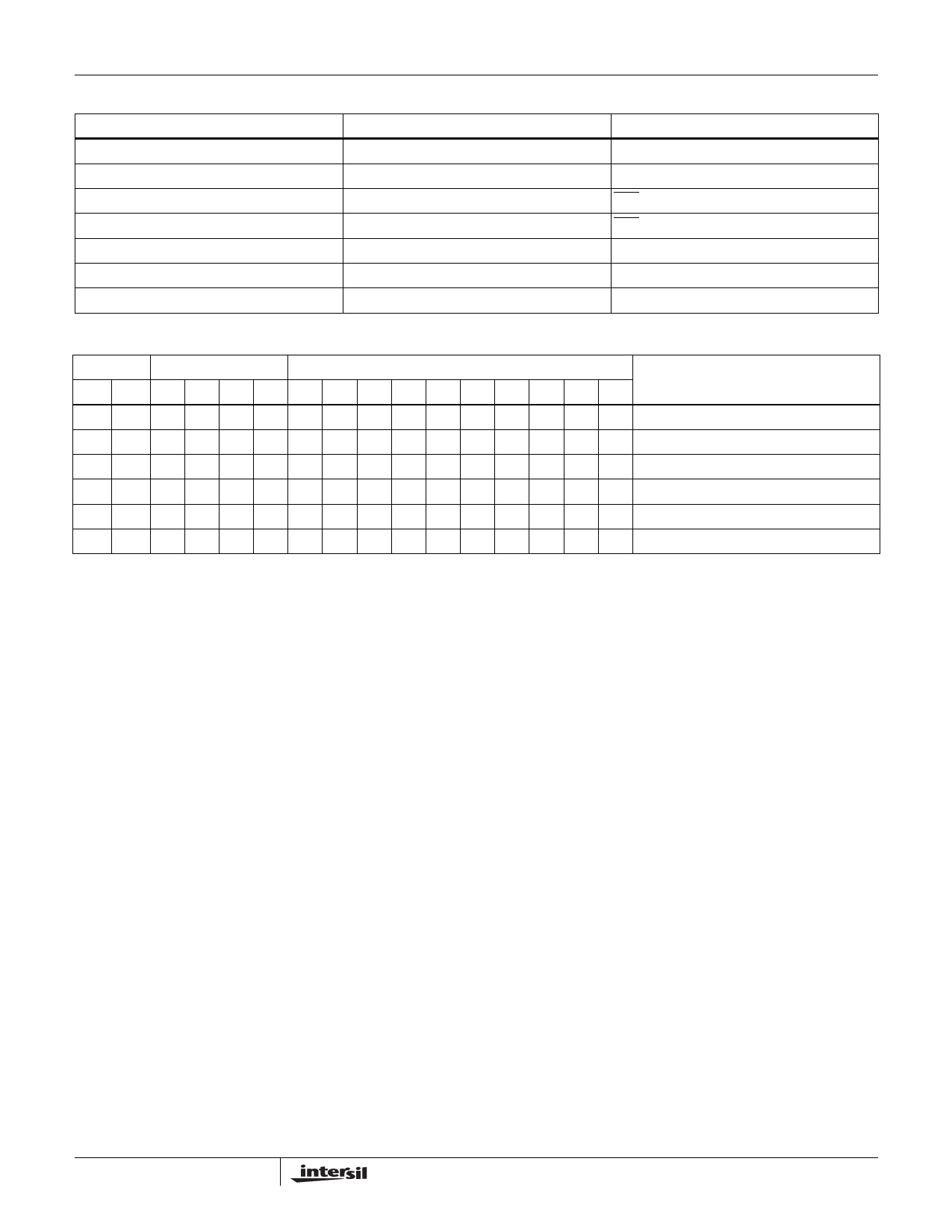
PARAMETER
T
tr/tf
tHE
tSE
tHD
tSD
tW
TABLE 2. SERIAL TIMING PARAMETERS
RECOMMENDED OPERATING RANGE
DESCRIPTION
≥200ns
Clock Period
0.05 * T
Clock Rise/Fall Time
≥10ns
ENA Hold Time
≥10ns
ENA Setup Time
≥10ns
Data Hold Time
≥10ns
Data Setup Time
0.50 * T
Clock Pulse Width
CONTROL CHANNEL ADDRESS
C1 C0 A3 A2 A1 A0 D9
0 0 00000
0 0 00001
0 0 00001
0 0 00111
0 0 01110
0 1 01110
TABLE 3. SERIAL PROGRAMMING EXAMPLES
DATA
D8 D7 D6 D5 D4 D3 D2 D1 D0
CONDITION
0 0 0 0 0 0 0 0 0 Internal Oscillator, Channel A, Value = 0
1 1 1 1 1 1 1 1 1 Internal Oscillator, Channel A, Value = 1023
0 0 0 0 0 0 0 0 0 Internal Oscillator, Channel A, Value = 512
0 0 0 0 0 0 0 0 1‘t Internal Oscillator, Channel C, Value = 513
0 0 0 0 1 1 1 1 1 Internal Oscillator, Channel H, Value = 31
0 0 0 0 1 1 1 1 1 External Oscillator, Channel H, Value = 31
Analog Section
TRANSFER FUNCTION
The transfer function is:
VOUT(IDEAL )
=
VREFL
+
-d---a----t--a--
1024
×
(VREFH
-
VREFL)
where data is the decimal value of the 10-bit data binary
input code.
The output voltages from the EL5325 will be derived from
the reference voltages present at the VREFL and VREFH
pins. The impedance between those two pins is about 32kΩ.
Care should be taken that the system design holds these two
reference voltages within the limits of the power rails of the
EL5325. GND < VREFH ≤ VS and GND ≤ VREFL ≤ VREFH.
In some LCD applications that require more than 12
channels, the system can be designed such that one
EL5325 will provide the Gamma correction voltages that are
more positive than the VCOM potential. The second EL5325
can provide the Gamma correction voltage more negative
than the VCOM potential. The Application Drawing shows a
system connected in this way.
CLOCK OSCILLATOR
The EL5325 requires an internal clock or external clock to
refresh its outputs. The outputs are refreshed at the falling OSC
clock edges. The output refreshed switches open at the rising
edges of the OSC clock. The driving load shouldn’t be changed
at the rising edges of the OSC clock. Otherwise, it will generate
a voltage error at the outputs. This clock may be input or output
via the clock pin labeled OSC. The internal clock is provided by
an internal oscillator running at approximately 21kHz and can
be output to the OSC pin. In a 2 chip system, if the driving loads
are stable, one chip may be programmed to use the internal
oscillator; then the OSC pin will output the clock from the
internal oscillator. The second chip may have the OSC pin
connected to this clock source.
For transient load application, the external clock Mode
should be used to ensure all functions are synchronized
together. The positive edge of the external clock to the OSC
pin should be timed to avoid the transient load effect. The
Application Drawing shows the LCD H rate signal used, here
the positive clock edge is timed to avoid the transient load of
the column driver circuits.
After power on, the chip will start with the internal oscillator
mode. At this time, the OSC pin will be in a high impedance
condition to prevent contention. By setting B14 to high, the
chip is on external clock mode. Setting B14 to low, the chip is
on internal clock mode.
7
Share Link: 