IS25F011A 데이터 시트보기 (PDF) - Integrated Silicon Solution
부품명
상세내역
제조사
IS25F011A
Integrated Silicon Solution

IS25F011A Datasheet PDF : 23 Pages
| |||
IS25F011A
IS25F021A
IS25F041A
ISSI ®
Following the byte-address field, 16 control clocks are
required with data=0. The Serial Data Output (SO) will
change from a high-impedance state and begin to drive
the output with Ready/Busy status RB[15:0]. If SO uses
the rising edge of clock (configuration register RCE=1),
the output will be driven after the last control clock. If
SO uses the falling edge of clock (RCE=0), the output
will be driven on the next falling edge of clock. If the
array is not busy, the output status will be 9999H,
followed by the sector data on the SO pin. If the array
is busy, the status will be 6666H, and the command
should be terminated and restarted after a ready state
occurs. The data field is shifted out with the least
significant byte first (i.e., byte-00H, byte-01H, ...). The
bit order within each byte is the most significant bit first
(i.e.,D7,...D0). The byte-address is internally incre-
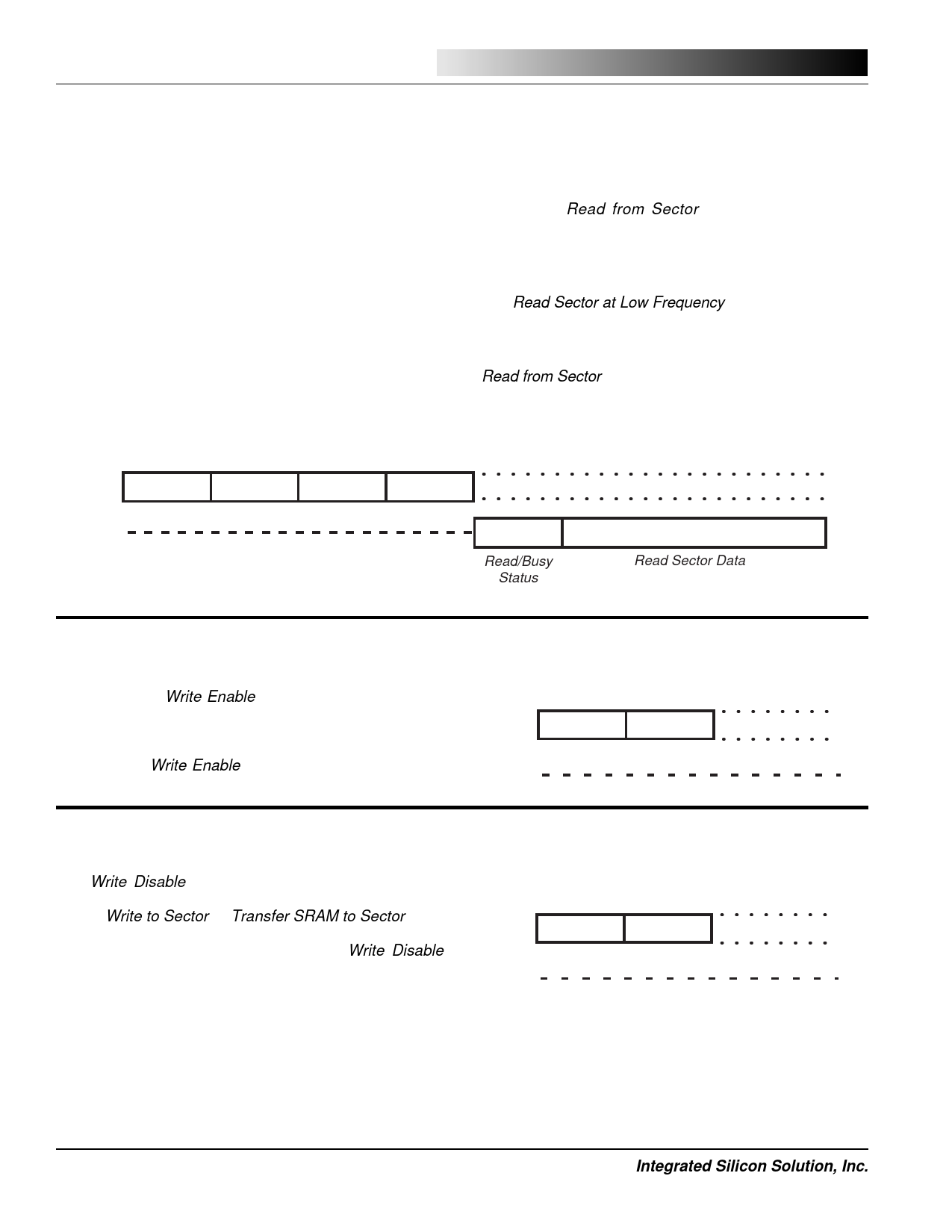
Read from
Sector
Command
Sector
Address*
Byte
Address** 16 Clocks
SI
52H
S[15:0]
B[15:0]
0000H
mented to the next higher byte address as the clock
continues. When the highest byte-address (107H) is
reached, the address counter rolls over to byte-0H and
continues to increment. Asserting the CS pin high
completes (or terminates) the command. Detailed tim-
ing for the Read from Sector command is shown in
Figure 10.
Read Sector (Low Frequency)
The Read Sector at Low Frequency command (51H) can
reduce power consumption during read operations by
25%-40% when the system clock frequency is 1 MHz or
lower. The command sequence is identical to the standard
Read from Sector command.
SO
*The sector address only uses bits [8:0], [9:0] or [10:0]
**The byte address only uses bits [8:0]
RB[15:0]
Read/Busy
Status
First Byte - Last Byte
Read Sector Data
Write Enable
Upon power-up, the Flash memory array is write- pro-
tected until the Write Enable command (06H) has been
issued. The WP pin must be inactive while writing the
command for the write enable to be accepted. The status
of the device’s write protect state can be read in the status
register. The Write Enable command sequence is com-
pleted by asserting CS high after eight additional clocks.
Write Enable
Command 8 Clocks
SI
06H
00H
SO
Write Disable
The Write Disable command (04H) protects the Flash
memory array from being programmed. Once issued,
further Write to Sector or Transfer SRAM to Sector com-
mands will be ignored. The status of the write protect state
can be read in the status register. The Write Disable
command sequence is completed by asserting CS high
after eight additional clocks.
Write Disable
Command 8 Clocks
SI
04H
00H
SO
12
Integrated Silicon Solution, Inc.
PRELIMINARY SF001-1A
06/24/98
Share Link: