IS25F011A 데이터 시트보기 (PDF) - Integrated Silicon Solution
부품명
상세내역
제조사
IS25F011A
Integrated Silicon Solution

IS25F011A Datasheet PDF : 23 Pages
| |||
IS25F011A
IS25F021A
IS25F041A
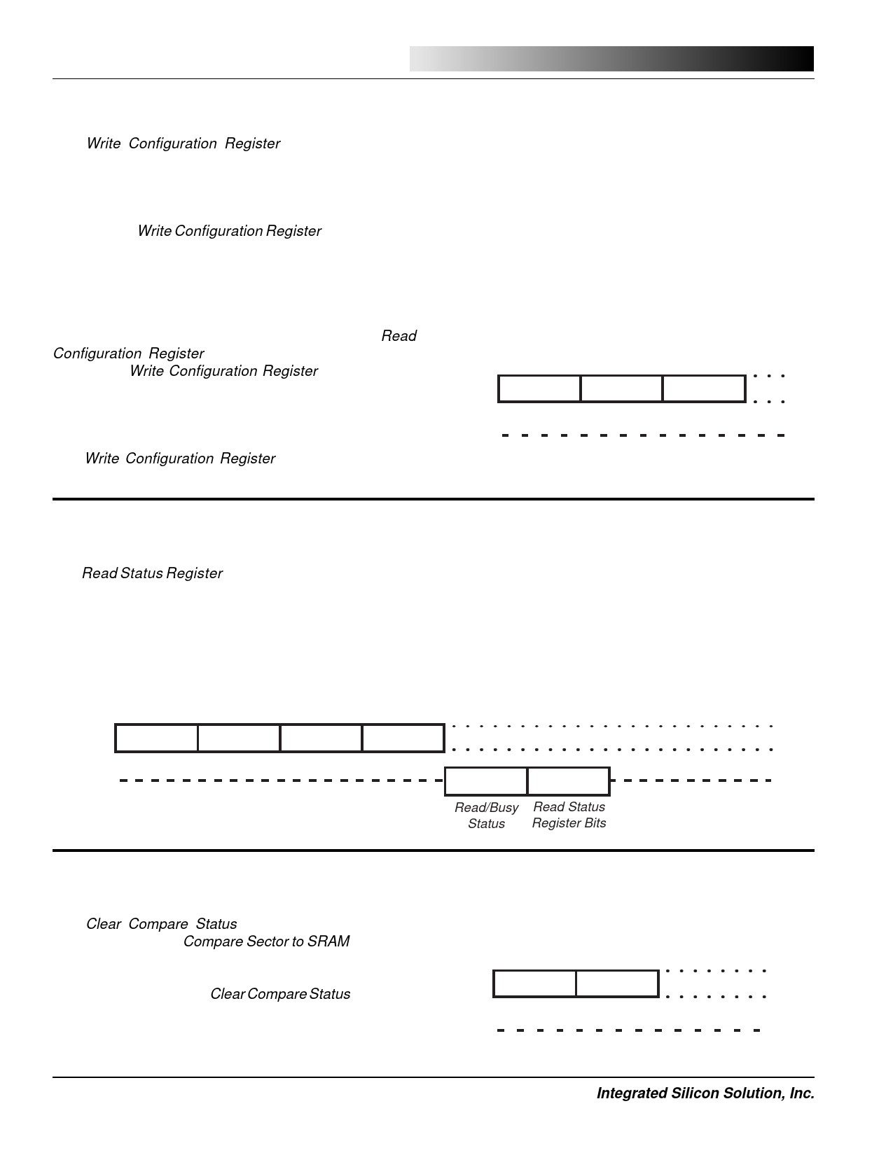
Write Configuration Register
The Write Configuration Register command provides
access to the configuration register which stores the
current configuration of the HOLD-R/B pin, read-data
clock edge, write protect range, and alternate oscillator
frequency. The configuration register is nonvolatile. Once
set using the Write Configuration Register command, the
contents will maintain even when power is removed.
Because the register’s state is stored in nonvolatile
memory, there is a finite endurance limit to the number of
times it can be written to. To limit the number of writes, it
is recommended that before writing to the configuration
register it should first be read from using the Read
Configuration Register command. If no change is re-
quired, the Write Configuration Register command can
be skipped. This process will help extend the endurance
of the configuration register bits and eliminate additional
programming “busy” time.
The Write Configuration Register command sequence
starts with the command byte (8AH) followed by a 16-bit
ISSI ®
field that specifies configuration register bit settings.
Although the field is 16-bits long, only bits CF[8:0] are
used. All other upper bits are reserved and must be
clocked using 0 for data. After an additional 16 control
clocks using 0 for data, the command can be completed
by asserting CS high. The device will become busy for a
short time (tWP) while the nonvolatile memory cells of the
configuration register are programmed.
Write
Configuration
Register Configuration
Command
Bits*
16 Clocks
SI
8AH
CF[15:0]
0000H
SO
*The CF Register only uses bits [8:0]
Read Status Register
The Read Status Register command provides access to
the status register and its status flags for Ready/Busy
(R/B), SRAM and program buffer transfer operations (TX),
Write Enable/Disable (WE), and Compare Not Equal (CNE)
(Figure 8). The command sequence is similar to the 0
command except that the sector address field S[15:0] and
the byte-address field B[15:0] are replaced by all 0 bits.
After 16 clocks and the Ready/Busy status field RB[15:0]
has been read, an 8-bit Status field ST[7:0] provides the
contents of the Status Register.
Read Status
Register
Command
16 Clocks
SI
83H
0000H
16 Clocks
0000H
16 Clocks
0000H
SO
RB[15:0]
ST[7:0]
Read/Busy Read Status
Status Register Bits
Clear Compare Status
The Clear Compare Status command (89H) works in
conjunction with the Compare Sector to SRAM command
and the Status Register. If any of the compared bits are not
equal, then the Compare Not Equal (CNE) bit in the Status
Register is set to a 1. The Clear Compare Status command
must be executed to reset the CNE bit to a 0.
Clear Compare
Status
Command 8 Clocks
SI
89H
00H
SO
18
Integrated Silicon Solution, Inc.
PRELIMINARY SF001-1A
06/24/98
Share Link: