F25L32PA-100PAG 데이터 시트보기 (PDF) - [Elite Semiconductor Memory Technology Inc.
부품명
상세내역
제조사
F25L32PA-100PAG
[Elite Semiconductor Memory Technology Inc.

F25L32PA-100PAG Datasheet PDF : 36 Pages
| |||
ESMT
F25L32PA
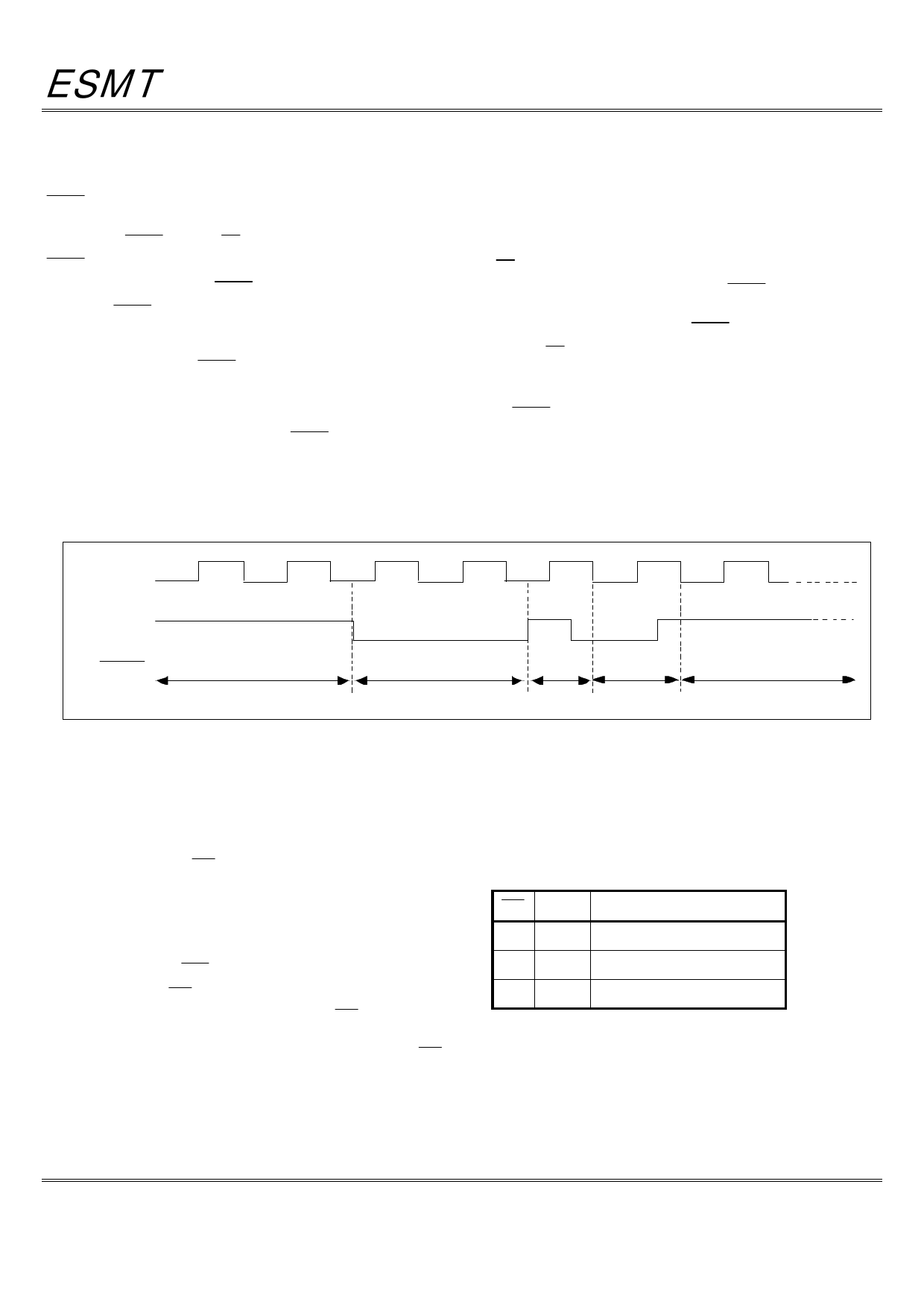
HOLD OPERATION
HOLD pin is used to pause a serial sequence underway with the
SPI flash memory without resetting the clocking sequence. To
activate the HOLD mode, CE must be in active low state. The
HOLD mode begins when the SCK active low state coincides
with the falling edge of the HOLD signal. The HOLD mode ends
when the HOLD signal’s rising edge coincides with the SCK
active low state.
If the falling edge of the HOLD signal does not coincide with the
SCK active low state, then the device enters Hold mode when the
SCK next reaches the active low state.
Similarly, if the rising edge of the HOLD signal does not
coincide with the SCK active low state, then the device exits in
Hold mode when the SCK next reaches the active low state. See
Figure 1 for Hold Condition waveform.
Once the device enters Hold mode, SO will be in high impedance
state while SI and SCK can be VIL or VIH.
If CE is driven active high during a Hold condition, it resets the
internal logic of the device. As long as HOLD signal is low, the
memory remains in the Hold condition. To resume
communication with the device, HOLD must be driven active
high, and CE must be driven active low. See Figure 23 for Hold
timing.
The HOLD function is only available for Standard and Dual SPI
operation.
SCK
HOLD
A ctive
Figure 1: HOLD Condition Waveform
Ho ld
A ctive
Ho ld
A ctive
WRITE PROTECTION
The device provides software Write Protection.
The Write-Protect pin ( WP ) enables or disables the lock-down
function of the status register. The Block-Protection bits (BP2,
BP1, BP0, and BPL) in the status register provide Write
protection to the memory array and the status register. See Table
4 for Block-Protection description.
Write Protect Pin ( WP )
The Write-Protect ( WP ) pin enables the lock-down function of
the BPL bit (bit 7) in the status register. When WP is driven low,
the execution of the Write Status Register (WRSR) instruction is
determined by the value of the BPL bit (see Table 4). When WP
is high, the lock-down function of the BPL bit is disabled.
Table 4: Conditions to Execute Write-Status- Register
(WRSR) Instruction
WP BPL Execute WRSR Instruction
L
1
Not Allowed
L
0
Allowed
H
X
Allowed
Elite Semiconductor Memory Technology Inc.
Publication Date: Mar. 2009
Revision: 1.0
11/36
Share Link: