HMS91C7134K 데이터 시트보기 (PDF) - Hynix Semiconductor
부품명
상세내역
제조사
HMS91C7134K Datasheet PDF : 90 Pages
| |||
HMS9xC7132 / HMS9xC7134
which the use of the stack starts) by using the initialization rou-
tine. Normally, the initial value of “07H” is used and the stack
area is 00H to 7FH .
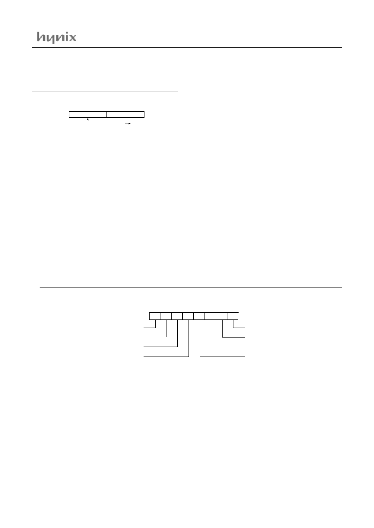
Stack Area (30H ~ 7FH)
Bit 15
87
00H
SP
Bit 0
Hardware fixed
00H~7FH
SP (Stack Pointer) could be in 00H~7FH.
Program Counter: The Program Counter is a 16-bit wide which
consists of two 8-bit registers, PCH and PCL. This counter indi-
cates the address of the next instruction to be executed. In reset
state, the program counter has reset routine address (PCH:0FFH,
PCL:0FEH).
Program Status Word: The Program Status Word (PSW) con-
tains several bits that reflect the current state of the CPU and se-
lect Internal RAM(00H~1FH:Bank0~Bank3). The PSW is
described in Figure 8-4. It contains the Carry flag, the Auxiliary
carry flag, the Half Carry (for BCD operation), the General pur-
pose flag, the Register bank select flags, the Overflow flag, the
undefined flag and Parity flag.
[Carry flag CY]
This flag stores any carry or not borrow from the ALU of CPU
after an arithmetic operation and is also changed by the Shift In-
struction or Rotate Instruction.
[Auxiliary carry flag AC]
After operation, this is set when there is a carry from bit 3 of ALU
or there is no borrow from bit 4 of ALU.
[Register bank select flags RS0, RS1]
This flags select one of four bank(00~07H:bank0, 08~0fH:bank1,
10~17H:bank2, 17~1FH:bank3)in Internal RAM.
[Overflow flag OV]
This flag is set to “1” when an overflow occurs as the result of an
arithmetic operation involving signs. An overflow occurs when
the result of an addition or subtraction exceeds +127(7FH) or -
128(80H). The CLRV instruction clears the overflow flag. There
is no set instruction. When the BIT instruction is executed, bit 6
of memory is copied to this flag.
[Parity flag P]
This flag reflect on number of Accumulator’s 1. If number of Ac-
uumulator’s 1 is odd, P=0. otherwise P=1. Sum of adding Acu-
umulator’s 1 to P is always even.
R0~R7: General purpose register.
Data Pointer Register:Data Pointer Register is 16-bit wide
which consists of two-8bit registers, DPH and DPL. This register
is used as a data pointer for the data transmission with external
data memory.
MSB
PSW CY AC F0 RS1 RS0 0V
CARRY FLAG
AUXILIARY CARRY FLAG
GENERAL PURPOSE FLAG
REGISTER BANK SELECT FLAG
(to select Bank0~3 with RS0)
LSB
P RESET VALUE: 00H
PARITY FLAG
NOT ASSIGNED BIT
OVERFLOW FLAG
REGISTER BANK SELECT FLAG
(to select Bank0~3 with RS1)
Figure 8-4 PSW(Program Status Word)Register
8.2 Program Memory
The program memory consists of ROM : 32K bytes (HMS91C7132) and 32K bytes (HMS97C7132)
8.3 Data memory
The internal data memory is divided into four physically separat-
ed part : 256 bytes of RAM, 256 bytes of XRAM0, and 128 bytes
of Special Function Registers (SFRs) areas.
RAM
Four register banks, each 8 registers wide, occupy locations 0
through 31 in the lower RAM area. Only one of these banks may
be enabled at a time. The next 16 bytes, locations 32 through 47,
May.2001 ver1.1
17
Share Link: 