LT5521 데이터 시트보기 (PDF) - Linear Technology
부품명
상세내역
제조사
LT5521 Datasheet PDF : 16 Pages
| |||
LT5521
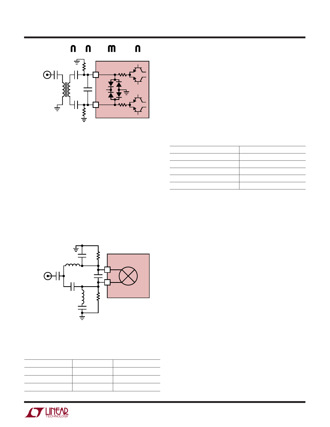
APPLICATIO S I FOR ATIO
C2
1nF R1 LT5521
IFIN
50Ω
T1
2:1
IN+
2
C13
VCC
1nF
IN–
3
R7
5521 F04
Figure 4. Low Frequency Signal Input
on the IF input frequency and the LO frequency. Smaller
C13 values have reduced impact on the LO output sup-
pression; larger values will degrade the conversion gain.
A single-ended 50Ω source can also be matched to the
differential signal inputs of the LT5521 without an input
transformer. Figure 5 shows an example topology for a
discrete balun, and Table 4 lists component values for
several frequencies. The discrete input match is intrinsi-
cally narrowband. LO suppression to the output is de-
graded and noise figure degrades by 4dB for input
frequencies greater than 200MHz. Noise figure degrada-
tion is worse at lower input frequencies.
C16
R1
110Ω
LT5521
L4
C2
82pF
IN+
2
IFIN
50Ω
C13
C14
IN–
3
L3
1nF
R7
110Ω
5521 F05
Figure 5. Alternative Transformerless Input Circuit
Using Low Cost Discrete Components
Table 4. Component Values for Discrete Bridge Balun Signal
Input Matching
IF (MHz)
C14, C16 (pF)
L3, L4 (nH)
220
22
22
250
18
18
640
4.7
4.7
Operation at Reduced Supply Voltage
External resistors R1 and R7 (Figure 2) set the current
through the mixer core. For best distortion performance,
these resistors should be chosen to maintain a total of
40mA through the mixer core (20mA per side). At 5V
supply, R1 and R7 should be 110Ω. Table 5 shows
recommended values for R1 and R7 at various supply
voltages. Caution: Using values below the recommended
resistance can adversely affect operation or damage the
part.
Table 5. Minimum External Resistor Values vs Supply Voltage
VCC (V)
5
R1, R7 (Ω)
110
4.5
82.5
4
54.9
3.5
38.3
3.3
23.2
Excessive mismatch between the external resistors R1
and R7 will degrade performance, particularly LO sup-
pression. Resistors with 1% mismatch are recommended
for optimum performance.
Figure 2 shows RF chokes in series with R1 and R7. These
inductors are optional. In general, the chokes improve the
conversion gain and noise figure by 2dB at 3.3V (i.e., at the
minimum values of R1 and R7). The DC resistance varia-
tion of the RF chokes must be considered in the 1% source
resistance mismatch suggested for maintaining LO sup-
pression performance.
Figure 6 indicates the typical performance of the LT5521
as the external source resistance (R1, R7) is varied while
keeping the supply current constant. Figure 6 data was
taken without the benefit of input chokes, and shows the
gradual gain degradation for smaller values of the input
resistors R1 and R7. Figure 7 shows the typical behavior
when the supply voltage is fixed and the core current is
varied by adjusting values of the external resistors R1 and
R7. Decreasing the core current decreases the power
consumption and improves noise figure but degrades
distortion performance. Figure␣ 8 demonstrates the im-
pact of the RF chokes in series with the source resistance
at 3.3V. There is a 2dB improvement in conversion gain
and noise figure and a corresponding decrease in IIP3.
5521f
11
Share Link: 