MT46H16M32LF 데이터 시트보기 (PDF) - Micron Technology
부품명
상세내역
제조사
MT46H16M32LF Datasheet PDF : 96 Pages
| |||
512Mb: x16, x32 Mobile LPDDR SDRAM
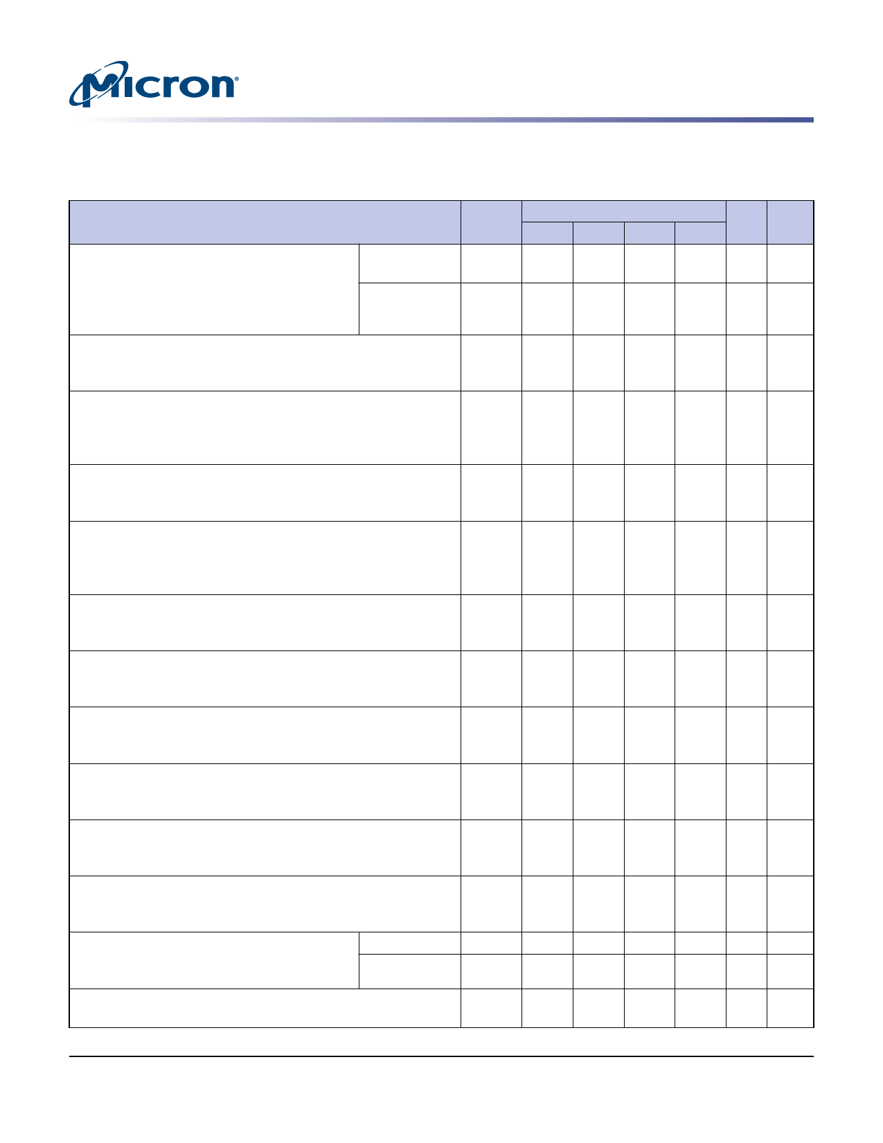
Electrical Specifications – IDD Parameters
Table 8: IDD Specifications and Conditions, –40°C to +85°C (x32)
Notes 1–5 apply to all the parameters/conditions in this table; VDD/VDDQ = 1.70–1.95V
Max
Parameter/Condition
Symbol -5
-54
-6
Operating 1 bank active precharge current: JEDEC-standard IDD0
70
65
60
tRC = tRC (MIN); tCK = tCK (MIN); CKE is HIGH; option
CS is HIGH between valid commands; Address Reduced page
inputs are switching every 2 clock cycles; Data size option
IDD0
70
65
60
bus inputs are stable
Precharge power-down standby current: All banks idle; CKE is
LOW; CS is HIGH; tCK = tCK (MIN); Address and control inputs
are switching; Data bus inputs are stable
IDD2P
300 300 300
Precharge power-down standby current: Clock stopped; All
IDD2PS
300
300
300
banks idle; CKE is LOW; CS is HIGH, CK = LOW, CK# = HIGH; Ad-
dress and control inputs are switching; Data bus inputs are sta-
ble
Precharge nonpower-down standby current: All banks idle; CKE IDD2N
15
15
15
= HIGH; CS = HIGH; tCK = tCK (MIN); Address and control inputs
are switching; Data bus inputs are stable
Precharge nonpower-down standby current: Clock stopped; All IDD2NS
8
8
8
banks idle; CKE = HIGH; CS = HIGH; CK = LOW, CK# = HIGH; Ad-
dress and control inputs are switching; Data bus inputs are sta-
ble
Active power-down standby current: 1 bank active; CKE = LOW; IDD3P
3
3
3
CS = HIGH; tCK = tCK (MIN); Address and control inputs are
switching; Data bus inputs are stable
Active power-down standby current: Clock stopped; 1 bank ac- IDD3PS
2
2
2
tive; CKE = LOW; CS = HIGH; CK = LOW; CK# = HIGH; Address
and control inputs are switching; Data bus inputs are stable
Active nonpower-down standby: 1 bank active; CKE = HIGH; CS IDD3N
15
15
15
= HIGH; tCK = tCK (MIN); Address and control inputs are switch-
ing; Data bus inputs are stable
Active nonpower-down standby: Clock stopped; 1 bank active; IDD3NS
8
8
8
CKE = HIGH; CS = HIGH; CK = LOW; CK# = HIGH; Address and
control inputs are switching; Data bus inputs are stable
Operating burst read: 1 bank active; BL = 4; CL = 3; tCK = tCK
IDD4R
115
110
105
(MIN); Continuous READ bursts; Iout = 0mA; Address inputs are
switching every 2 clock cycles; 50% data changing each burst
Operating burst write: One bank active; BL = 4; tCK = tCK
IDD4W
115
110
105
(MIN); Continuous WRITE bursts; Address inputs are switching;
50% data changing each burst
Auto refresh: Burst refresh; CKE = HIGH; Ad- tRFC = 138ns
IDD5
95
95
95
dress and control inputs are switching; Data
bus inputs are stable
tRFC = tREFI
IDD5A
3
3
3
Deep power-down current: Address and control pins are stable; IDD8
10
10
10
Data bus inputs are stable
-75 Unit Notes
50 mA 6
50 mA 6
300 μA 7, 8
300 μA
7
12 mA 9
8 mA 9
3 mA 8
2 mA
15 mA 6
8 mA 6
100 mA 6
100 mA 6
95 mA 10
3 mA 10, 11
10 μA 7, 13
PDF: 09005aef83dd2b3e
t67m_512mb_mobile_lpddr.pdf - Rev. H 06/13 EN
21
Micron Technology, Inc. reserves the right to change products or specifications without notice.
© 2009 Micron Technology, Inc. All rights reserved.
Share Link: 