EL5111T 데이터 시트보기 (PDF) - Renesas Electronics
부품명
상세내역
제조사
EL5111T Datasheet PDF : 14 Pages
| |||
EL5111T
Applications Information
Product Description
The EL5111T is a high voltage rail-to-rail input-output
amplifier with low power consumption. The EL5111T is
a single amplifier which exhibits beyond the rail input
capability, rail-to-rail output capability, and is unity gain
stable.
The EL5111T features a high slew rate of 100V/µs, and
fast settling time. Also, the device provides common
mode input capability beyond the supply rails,
rail-to-rail output capability, and a bandwidth of 60MHz
(-3dB). This enables the amplifier to offer maximum
dynamic range at any supply voltage.
Operating Voltage, Input and Output
Capability
The EL5111T can operate on a single supply or dual
supply configuration. The EL5111T operating voltage
ranges from a minimum of 4.5V to a maximum of 19V.
This range allows for a standard 5V (or ±2.5V) supply
voltage to dip to -10%, or a standard 18V (or ±9V) to
rise by +5.5% without affecting performance or
reliability.
The input common-mode voltage range of the EL5111T
extends 500mV beyond the supply rails. Also, the
EL5111T is immune to phase reversal. However, if the
common mode input voltage exceeds the supply
voltage by more than 0.5V, electrostatic protection
diodes in the input stage of the device begin to
conduct. Even though phase reversal will not occur, to
maintain optimal reliability it is suggested to avoid
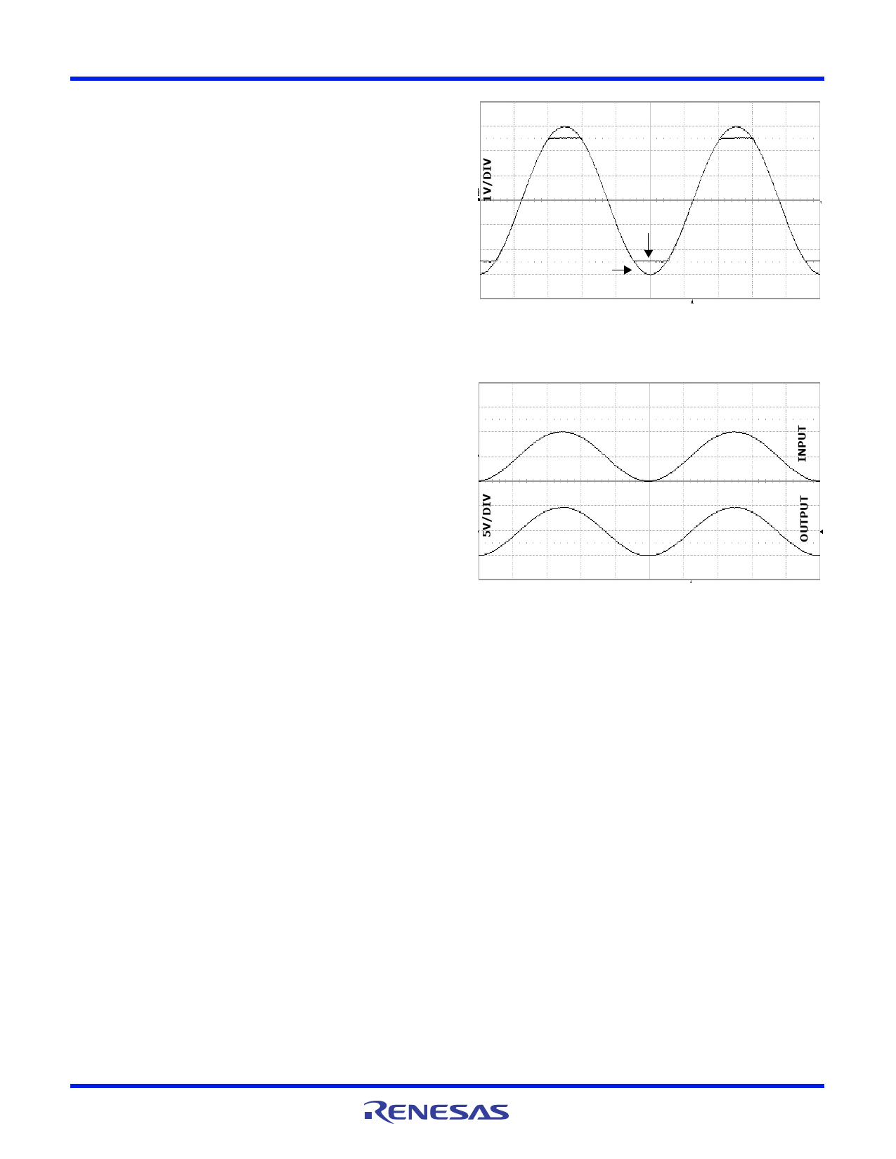
input overvoltage conditions. Figure 30 shows the input
voltage driven 500mV beyond the supply rails and the
device output swinging between the supply rails.
The EL5111T output typically swings to within 50mV of
positive and negative supply rails with load currents of
±5mA. Decreasing load currents will extend the output
voltage range even closer to the supply rails. Figure 31
shows the input and output waveforms for the device
in a unity-gain configuration. Operation is from ±5V
supply with a 1k load connected to GND. The input is
a 10VP-P sinusoid and the output voltage is
approximately 9.9VP-P.
Refer to the “Electrical Specifications” Table beginning
on page 3 for specific device parameters. Parameter
variations with operating voltage, loading and/or
temperature are shown in the “Typical Performance
Curves” on page 6.
VS = ±2.5V, TA = +25°C, AV = 1, VINx = 6VP-P,
RL = 1kto GND
OUTPUT
INPUT
10µs/DIV
FIGURE 30. OPERATION WITH BEYOND-THE-RAILS
INPUT
VS = ±5V, TA = +25°C, AV = 1, VINx = 10VP-P,
RL = 1kto GND
10µs/DIV
FIGURE 31. OPERATION WITH RAIL-TO-RAIL INPUT
AND OUTPUT
Output Current
The EL5111T is capable of output short circuit currents
of 300mA (source and sink), and the device has
built-in protection circuitry which limits the output
current to ±300mA (typical).
To maintain maximum reliability, the continuous output
current should never exceed ±70mA. This ±70mA limit
is determined by the characteristics of the internal
metal interconnects. Also, see “Power Dissipation” on
page 12 for detailed information on ensuring proper
device operation and reliability for temperature and
load conditions.
Thermal Shutdown
The EL5111T has a built-in thermal protection which
ensures safe operation and prevents internal damage
to the device due to overheating. When the die
temperature reaches +165°C (typical) the device
automatically shuts OFF the output by putting it in a
high impedance state. When the die cools by +15°C
(typical) the device automatically turns ON the output
by putting it in a low impedance (normal) operating
state.
FN6894 Rev 0.00
May 27, 2010
Page 11 of 14
Share Link: 