MT28F002B3 데이터 시트보기 (PDF) - Micron Technology
부품명
상세내역
제조사
MT28F002B3 Datasheet PDF : 31 Pages
| |||
2Mb
SMART 3 BOOT BLOCK FLASH MEMORY
COMMAND EXECUTION
Commands are issued to bring the device into differ-
ent operational modes. Each mode allows specific op-
erations to be performed. Several modes require a
sequence of commands to be written before they are
reached. The following section describes the properties
of each mode, and Table 3 lists all command sequences
required to perform the desired operation.
READ ARRAY
The array read mode is the initial state of the device
upon power-up and after a RESET. If the device is in any
other mode, READ ARRAY (FFH) must be given to
return to the array read mode. Unlike the WRITE SETUP
command (40H), READ ARRAY does not need to be
given before each individual read access.
IDENTIFY DEVICE
IDENTIFY DEVICE (90H) may be written to the CEL
to enter the identify device mode. While the device is
in this mode, any READ will produce the device ID
when A0 is HIGH and manufacturer compatibility ID
when A0 is LOW. The device will remain in this mode
until another command is given.
WRITE SEQUENCE
Two consecutive cycles are needed to write data to
the array. WRITE SETUP (40H or 10H) is given in the
first cycle. The next cycle is the WRITE, during which
the write address and data are issued and VPP is brought
to VPPH. Writing to the boot block also requires that the
RP# pin be brought to VHH or that the WP# pin be
brought HIGH at the same time VPP is brought to VPPH.
The ISM will now begin to write the word or byte. VPP
must be held at VPPH until the WRITE is completed
(SR7 = 1).
While the ISM executes the WRITE, the ISM status
bit (SR7) will be at “0,” and the device will not respond
to any commands. Any READ operation will produce
the status register contents on DQ0-DQ7. When the
ISM status bit (SR7) is set to a logic 1, the WRITE has
been completed, and the device will go into the status
register read mode until another command is given.
After the ISM has initiated the WRITE, it cannot be
aborted except by a RESET or by powering down the
part. Doing either during a WRITE will corrupt the data
being written. If only the WRITE SETUP command has
been given, the WRITE may be nullified by performing
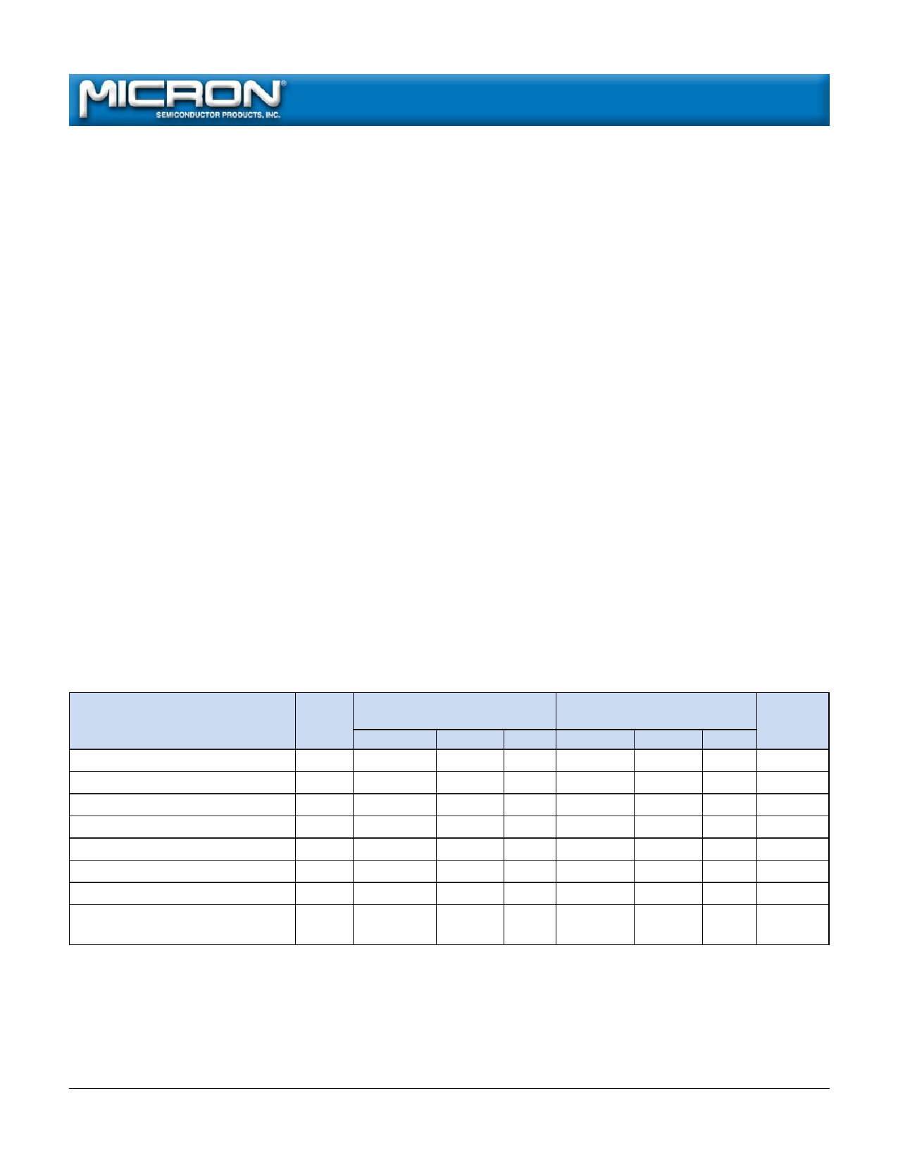
Table 3
Command Sequences
COMMANDS
READ ARRAY
IDENTIFY DEVICE
READ STATUS REGISTER
CLEAR STATUS REGISTER
ERASE SETUP/CONFIRM
ERASE SUSPEND/RESUME
WRITE SETUP/WRITE
ALTERNATE WORD/BYTE
WRITE
BUS
1ST
2ND
CYCLES
CYCLE
CYCLE
REQ’D OPERATION ADDRESS DATA OPERATION ADDRESS DATA
1
WRITE
X
FFH
3
WRITE
X
90H
READ
IA
ID
2
WRITE
X
70H
READ
X
SRD
1
WRITE
X
50H
2
WRITE
X
20H WRITE
BA
D0H
2
WRITE
X
B0H WRITE
X
D0H
2
WRITE
X
40H WRITE
WA
WD
2
WRITE
X
10H WRITE
WA
WD
NOTES
1
2, 3
4
5, 6
6, 7
6, 7
NOTE: 1. Must follow WRITE or ERASE CONFIRM commands to the CEL in order to enable flash array READ cycles.
2. IA = Identify Address: 00H for manufacturer compatibility ID; 01H for device ID.
3. ID = Identify Data.
4. SRD = Status Register Data.
5. On x16 (X00) devices BA = Block Address (A12-A16), on x8 (00X) devices BA = Block Address (A13-A16/A17).
6. Addresses are “Don’t Care” in first cycle but must be held stable.
7. WA = Address to be written; WD = Data to be written to WA.
2Mb Smart 3 Boot Block Flash Memory
F48.p65 – Rev. 1/00
12
Micron Technology, Inc., reserves the right to change products or specifications without notice.
©2000, Micron Technology, Inc.
Share Link: 