OR4E10 데이터 시트보기 (PDF) - Agere -> LSI Corporation
부품명
상세내역
제조사
OR4E10 Datasheet PDF : 124 Pages
| |||
Preliminary Data Sheet
December 2000
ORCA Series 4 FPGAs
Programmable Logic Cells (continued)
Look-Up Table Operating Modes
The operating mode affects the functionality of the PFU input and output ports and internal PFU routing. For exam-
ple, in some operating modes, the DIN[7:0] inputs are direct data inputs to the PFU latches/FFs. In memory mode,
the same DIN[7:0] inputs are used as a 4-bit write data input bus and a 4-bit write address input bus
into LUT memory.
Table 3 lists the basic operating modes of the LUT. Figure 4—Figure 7 show block diagrams of the LUT operating
modes. The accompanying descriptions demonstrate each mode’s use for generating logic.
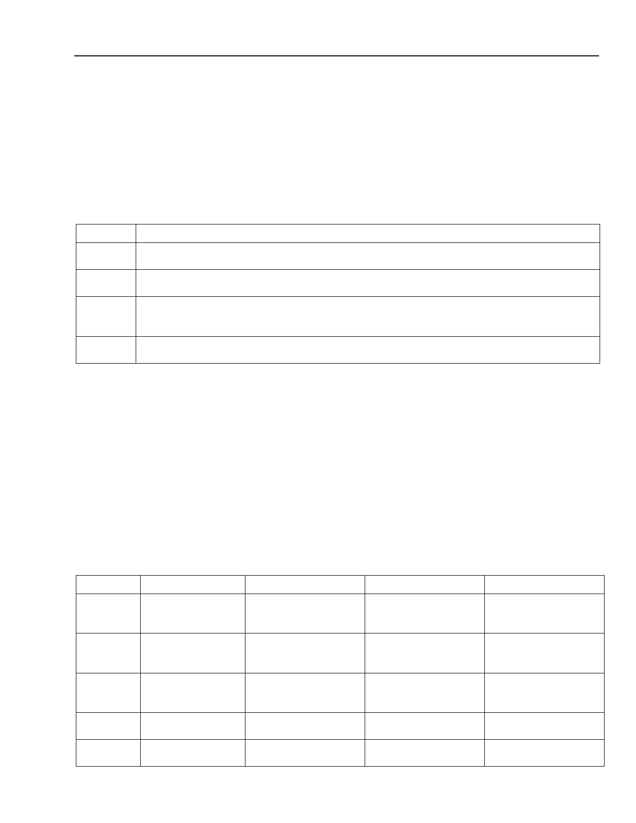
Table 3. Look-Up Table Operating Modes
Mode
Function
Logic
4-, 5-, and 6-input LUTs; softwired LUTs; latches/FFs with direct input or LUT input; CIN as direct
input to ninth FF or as pass through to COUT.
Half Logic/ Upper four LUTs and latches/FFs in logic mode; lower four LUTs and latches/FFs in ripple mode;
Half Ripple CIN and ninth FF for logic or ripple functions.
Ripple
All LUTs combined to perform ripple-through data functions. Eight LUT registers available for
direct-in use or to register ripple output. Ninth FF dedicated to ripple out, if used. The submodes of
ripple mode are adder/subtractor, counter, multiplier, and comparator.
Memory All LUTs and latches/FFs used to create a 32x4 synchronous dual-port RAM. Can be used as
single-port or as ROM.
PFU Control Inputs
Each PFU has eight routable control inputs and an active-low, asynchronous global set/reset (GSRN) signal that
affects all latches and FFs in the device. The eight control inputs are CLK[1:0], LSR[1:0], CE[1:0], and SEL[1:0],
and their functionality for each logic mode of the PFU is shown in Table 4. The clock signal to the PFU is CLK, CE
stands for clock enable, which is its primary function. LSR is the local set/reset signal that can be configured as syn-
chronous or asynchronous. The selection of set or reset is made for each latch/FF and is not a function of the signal
itself. SEL is used to dynamically select between direct PFU input and LUT output data as the input to
the latches/FFs.
All of the control signals can be disabled and/or inverted via the configuration logic. A disabled clock enable
indicates that the clock is always enabled. A disabled LSR indicates that the latch/FF never sets/resets (except from
GSRN). A disabled SEL input indicates that DIN[7:0] PFU inputs or the LUT outputs are always input to the latches/
FFs.
Table 4. Control Input Functionality
Mode
CLK[1:0]
LSR[1:0]
Logic
CLK to all latches/
FFs
LSR to all latches/FFs,
enabled per nibble and
for ninth FF
Half Logic/ CLK to all latches/
Half Ripple FFs
LSR to all latches/FF,
enabled per nibble and
for ninth FF
Ripple
CLK to all latches/
FFs
LSR to all latches/FFs,
enabled per nibble and
for ninth FF
Memory CLK to RAM
(RAM)
LSR0 port enable 2
Memory Optional for
Not used
(ROM) synchronous outputs
CE[1:0]
CE to all latches/FFs,
selectable per nibble
and for ninth FF
CE to all latches/FFs,
selectable per nibble
and for ninth FF
CE to all latches/FFs,
selectable per nibble
and for ninth FF
CE1 RAM write enable
CE0 Port enable 1
Not used
SEL[1:0]
Select between LUT
input and direct input for
eight latches/FFs
Select between LUT
input and direct input for
eight latches/FFs
Select between LUT
input and direct input for
eight latches/FFs
Not used
Not used
Lucent Technologies Inc.
11
Share Link: 