S3C1860 데이터 시트보기 (PDF) - Samsung
부품명
상세내역
제조사
S3C1860 Datasheet PDF : 91 Pages
| |||
S3C1840
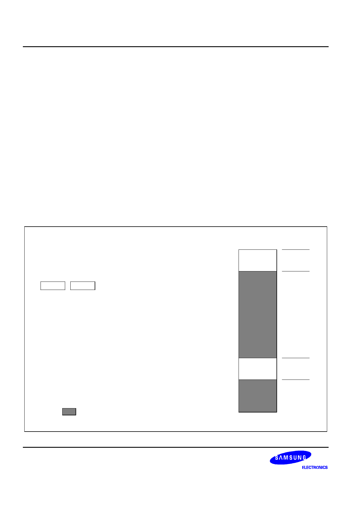
DATA MEMORY (RAM)
The S3C1840's data memory consists of a 32-nibble RAM which is organized into two files of 16 nibbles each
(See Figure 1-11).
RAM addressing is implemented by a 7-bit register, HL.
It's upper 3-bit register (H) selects one of two files and its lower 4-bit register (L) selects one of 16 nibbles in the
selected file.
Instructions which manipulate the H and L registers are as follow:
Select a file :
MOV
NOT
H,#n
H
; H ← #n, where n must be 0,4
; Complement MSB of H register
Select a nibble in a selected file :
MOV
MOV
MOV
INCS
DECS
L,A
L,A,@HL
L,#N
L
L
; L←A
; L ← M (H,L)
; L ← #n, where 0 ≤ n ≤ 0FH
; L←L+1
; L←L-1
H
L
3-bit
4-bit
The 7-bit HL register pair points to one of the 32 nibbles.
H register selects one of two files; 0, 4
L register selects one of 16 nibbles; 0 to 0FH
After reset, the HL register pair becomes to unknown state.
RAM Address
00
0F
File 0
40
File 4
4F
: Not built-in chip
7F
Figure 1-11. S3C1840 Data Memory Map
1-10
Share Link: 