LC66354C 데이터 시트보기 (PDF) - SANYO -> Panasonic
부품명
상세내역
제조사
LC66354C Datasheet PDF : 21 Pages
| |||
LC66354C, 66356C, 66358C
Continued from preceding page.
Parameter
Symbol
Conditions
min
typ
max
Unit Note
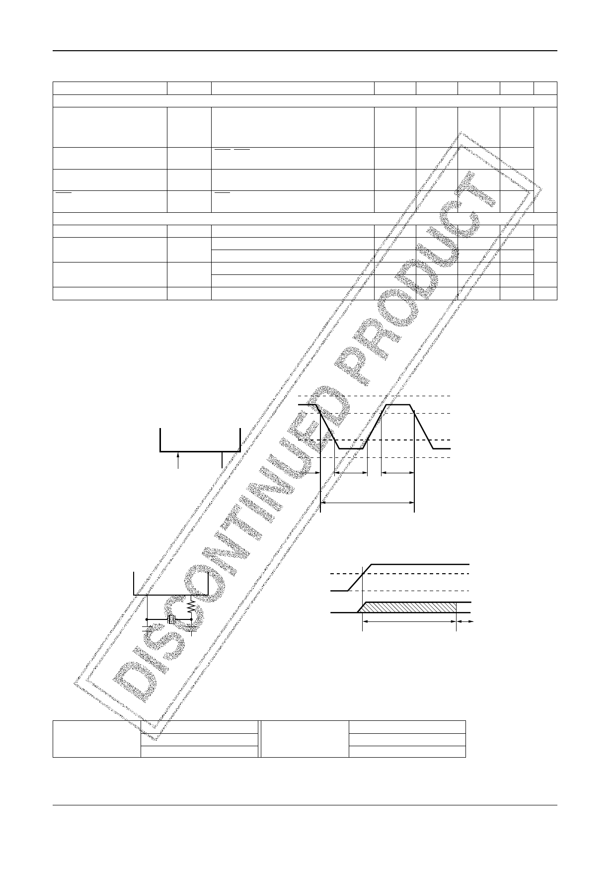
[Pulse conditions]
INT0 high and low-level
INT0: Figure 6, conditions under which the INT0
interrupt can be accepted, conditions under
tIOH, tIOL which the timer 0 event counter or pulse width
2
measurement input can be accepted
Tcyc
High and low-level pulse widths
INT1, INT2: Figure 6, conditions under which
for interrupt inputs other than INT0 tIIH, tIIL the corresponding interrupt can be accepted
2
Tcyc
PIN1 high and low-level
pulse widths
PIN1: Figure 6, conditions under which the
tPINH, tPINL timer 1 event counter input can be accepted
2
Tcyc
RES high and low-level
pulse widths
RES: Figure 6, conditions under which reset
tRSH, tRSL can be applied.
3
Tcyc
Comparator response speed
TRS
PD: Figure 7, VDD = 3.0 to 5.5 V
20
ms
Operating current drain
IDD OP
VDD: 4-MHz ceramic oscillator
VDD: 4-MHz external clock
3.0
5.0
mA
6
3.0
5.0
mA
Halt mode current drain
IDDHALT
VDD: 4-MHz ceramic oscillator
VDD: 4-MHz external clock
1.0
2.0
mA
1.0
2.0
mA
Hold mode current drain
IDDHOLD VDD: VDD = 1.8 to 5.5 V
0.01
10
µA
Note: 1. With the output Nch transistor off in shared I/O ports with the open-drain output specifications. These pins cannot be used as input pins if the
CMOS output specifications are selected.
2. With the output Nch transistor off in shared I/O ports with the open-drain output specifications. The rating for the pull-up output specification pins is
stipulated in terms of the output pull-up current IPO. These pins cannot be used as input pins if the CMOS output specifications are selected.
3. With the output Nch transistor off for CMOS output specification pins.
4. With the output Nch transistor off for pull-up output specification pins.
5. With the output Nch transistor off for open-drain output specification pins.
6. Reset state
VDD
0.8VDD
OSC1 (OSC2)
0.2VDD
External clock OPEN
textL
textH
VSS
textF
textR
1/fext
Figure 1 External Clock Input Waveform
VDD
OSC1
OSC2
Rd
C1 Ceramic C2
oscillator
OSC
Oscillator
unstable period
tCFS
Operating VDD
minimum value
0V
Stable oscillation
Figure 2 Ceramic Oscillator Circuit
Figure 3 Oscillator Stabilization Period
Table 1 Guaranteed Ceramic Oscillator Constants
4 MHz
(Murata Mfg. Co., Ltd.)
CSA4.00MG
C1 = 33 pF ± 10%
C2 = 33 pF ± 10%
Rd = 0
4 MHz
(Kyocera Corporation)
KBR4.0MS
C1 = 33 pF ± 10%
C2 = 33 pF ± 10%
Rd = 0
No. 5484-11/21
Share Link: 