MT48H16M16LFF-8 데이터 시트보기 (PDF) - Micron Technology
부품명
상세내역
제조사
MT48H16M16LFF-8 Datasheet PDF : 58 Pages
| |||
READs
READ bursts are initiated with a READ command,
as shown in Figure 5.
The starting column and bank addresses are pro-
vided with the READ command, and auto precharge is
either enabled or disabled for that burst access. If auto
precharge is enabled, the row being accessed is
precharged at the completion of the burst. For the ge-
neric READ commands used in the following illustra-
tions, auto precharge is disabled.
During READ bursts, the valid data-out element
from the starting column address will be available fol-
lowing the CAS latency after the READ command. Each
subsequent data-out element will be valid by the next
positive clock edge. Figure 6 shows general timing for
each possible CAS latency setting.
ADVANCE
256Mb: x16
MOBILE SDRAM
Upon completion of a burst, assuming no other com-
mands have been initiated, the DQs will go High-Z. A
full-page burst will continue until terminated. (At the
end of the page, it will wrap to the start address and
continue.)
Data from any READ burst may be truncated with a
subsequent READ command, and data from a fixed-
length READ burst may be immediately followed by
data from a READ command. In either case, a continu-
ous flow of data can be maintained. The first data ele-
ment from the new burst follows either the last ele-
ment of a completed burst or the last desired data ele-
ment of a longer burst that is being truncated. The new
READ command should be issued x cycles before the
clock edge at which the last desired data element is
valid, where x equals the CAS latency minus one.
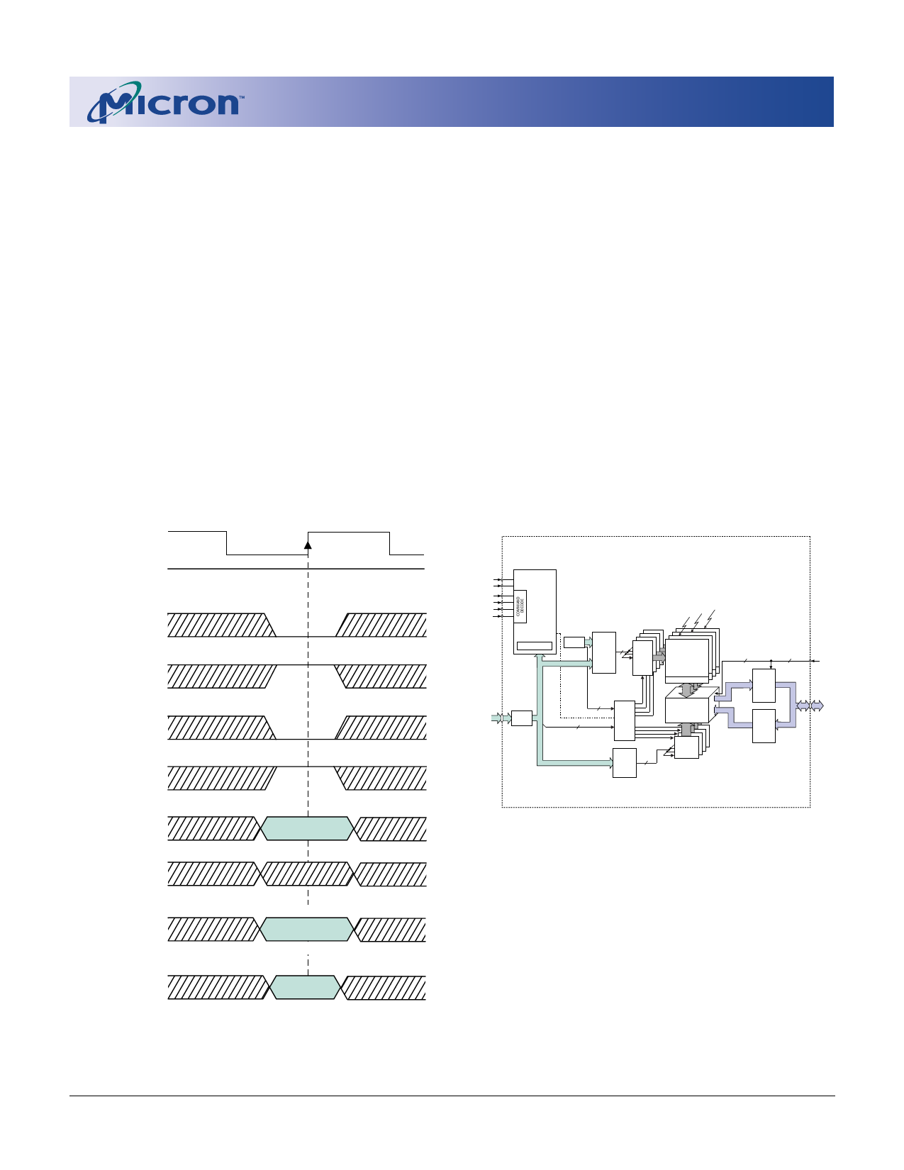
Figure 5
READ Command
CLK
CKE HIGH
CS#
RAS#
CAS#
WE#
A0-A8: x16
A9, A11: x16
A10
BA0,1
COLUMN
ADDRESS
ENABLE AUTO PRECHARGE
DISABLE AUTO PRECHARGE
BANK
ADDRESS
Figure 6
CAS Latency
CKE
CLK
CS#
WE#
CAS#
RAS#
CONTROL
LOGIC
BANK3
BANK2
BANK1
MODE REGISTER
12
A0-A12,
BA0, BA1
15
ADDRESS
REGISTER
REFRESH 13
COUNTER
ROW-
13
ADDRESS
MUX
13
BANK0
ROW-
ADDRESS
LATCH
&
DECODER
8192
BANK0
MEMORY
ARRAY
(8,192 x 256 x 32)
SENSE AMPLIFIERS
8192
2
BANK
CONTROL
LOGIC
2
COLUMN-
ADDRESS
8
8
COUNTER/
LATCH
I/O GATING
DQM MASK LOGIC
READ DATA LATCH
WRITE DRIVERS
256
(x32)
COLUMN
DECODER
4
4
DATA
32
OUTPUT
REGISTER
32
DATA
32
INPUT
REGISTER
DQM0-
DQM3
DQ0-
DQ31
256Mb: x16 Mobile SDRAM
MobileRamY26L_A.p65 – Pub. 5/02
15
Micron Technology, Inc., reserves the right to change products or specifications without notice.
©2002, Micron Technology, Inc.
Share Link: 