MT48H16M16LFF-8 데이터 시트보기 (PDF) - Micron Technology
부품명
상세내역
제조사
MT48H16M16LFF-8 Datasheet PDF : 58 Pages
| |||
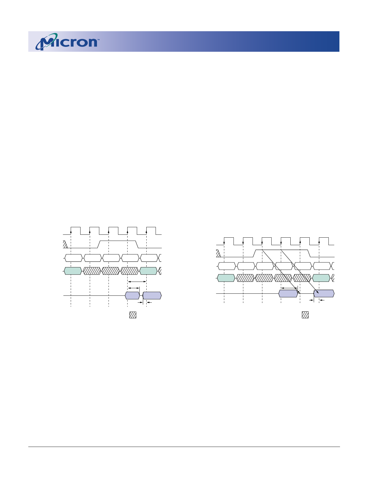
Data from any READ burst may be truncated with a
subsequent WRITE command, and data from a fixed-
length READ burst may be immediately followed by
data from a WRITE command (subject to bus turn-
around limitations). The WRITE burst may be initiated
on the clock edge immediately following the last (or last
desired) data element from the READ burst, provided
that I/O contention can be avoided. In a given system
design, there may be a possibility that the device driv-
ing the input data will go Low-Z before the SDRAM DQs
go High-Z. In this case, at least a single-cycle delay
should occur between the last read data and the WRITE
command.
The DQM input is used to avoid I/O contention, as
shown in Figures 9 and 10. The DQM signal must be
asserted (HIGH) at least two clocks prior to the WRITE
command (DQM latency is two clocks for output
ADVANCE
256Mb: x16
MOBILE SDRAM
buffers) to suppress data-out from the READ. Once the
WRITE command is registered, the DQs will go High-Z
(or remain High-Z), regardless of the state of the DQM
signal; provided the DQM was active on the clock just
prior to the WRITE command that truncated the READ
command. If not, the second WRITE will be an invalid
WRITE. For example, if DQM was LOW during T4 in
Figure 10, then the WRITEs at T5 and T7 would be
valid, while the WRITE at T6 would be invalid.
The DQM signal must be de-asserted prior to the
WRITE command (DQM latency is zero clocks for input
buffers) to ensure that the written data is not masked.
Figure 9 shows the case where the clock frequency al-
lows for bus contention to be avoided without adding a
NOP cycle, and Figure 10 shows the case where the
additional NOP is needed.
Figure 9
READ to WRITE
T0
T1
T2
T3
T4
CLK
DQM
COMMAND
READ
NOP
NOP
NOP
WRITE
ADDRESS
BANK,
COL n
DQ
tCK
tHZ
BANK,
COL b
DOUT n
DIN b
tDS
DON’T CARE
NOTE:
A CAS latency of three is used for illustration. The READ
command may be to any bank, and the WRITE command
may be to any bank. If a burst of one is used, then DQM is
not required.
Figure 10
READ to WRITE With
Extra Clock Cycle
T0
T1
T2
T3
CLK
DQM
T4
T5
COMMAND
READ
NOP
NOP
NOP
NOP
WRITE
ADDRESS
BANK,
COL n
DQ
tHZ
DOUT n
BANK,
COL b
DIN b
tDS
DON’T CARE
NOTE: A CAS latency of three is used for illustration. The READ command
may be to any bank, and the WRITE command may be to any bank.
256Mb: x16 Mobile SDRAM
MobileRamY26L_A.p65 – Pub. 5/02
18
Micron Technology, Inc., reserves the right to change products or specifications without notice.
©2002, Micron Technology, Inc.
Share Link: 