MT46H16M16 데이터 시트보기 (PDF) - Micron Technology
부품명
상세내역
제조사
MT46H16M16 Datasheet PDF : 79 Pages
| |||
256Mb: x16, x32 Mobile DDR SDRAM
Register Definition
Operating Mode
The normal operating mode is selected by issuing a LOAD MODE REGISTER command
with bits A7–A11 (x32) or A7–A12 (x16) each set to zero and bits A0–A6 set to the desired
values.
All other combinations of values for A7–A11/A12 are reserved for future use and/or test
modes. Test modes and reserved states should not be used, because unknown operation
or incompatibility with future versions may result.
Extended Mode Register
The extended mode register controls functions specific to Mobile SDRAM operation.
These additional functions include drive strength, temperature-compensated self
refresh, and partial-array self refresh.
The extended mode register is programmed via the LOAD MODE REGISTER command
(with BA0 = 0 and BA1 = 1) and will retain the stored information until it is programmed
again, the device goes into deep power-down mode, or the device loses power.
Temperature-Compensated Self Refresh
On this version of the Mobile DDR SDRAM, a temperature sensor is implemented for
automatic control of the SELF REFRESH oscillator. Programming the TCSR bits will have
no effect on the device. The SELF REFRESH oscillator will continue to refresh at the
factory-programmed optimal rate for the device temperature.
Partial-Array Self Refresh
For further power savings during SELF REFRESH, the partial-array self refresh (PASR)
feature enables the controller to select the amount of memory that will be refreshed
during SELF REFRESH.
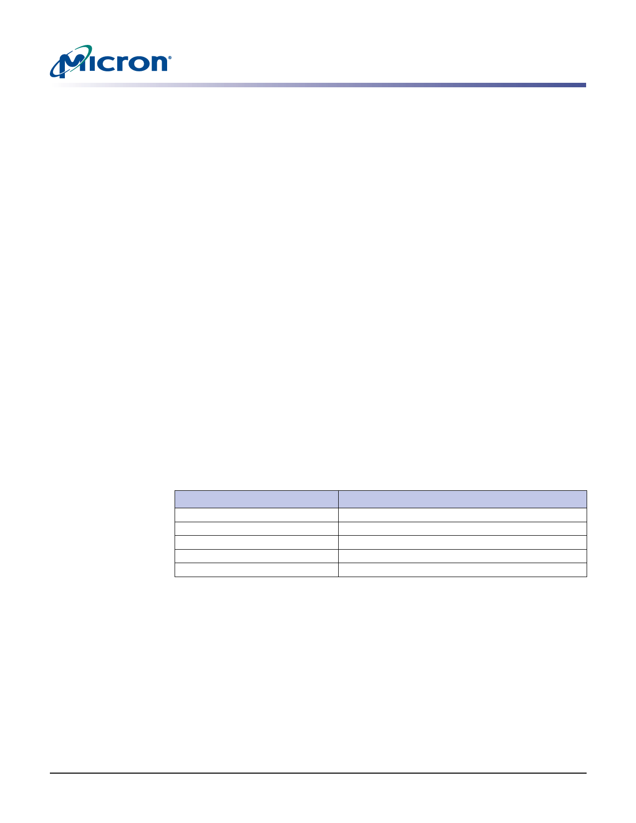
Table 6: Partial-Array Self Refresh Options
Memory
Full array
Half array
Quarter array
Eighth array
Sixteenth array
Bank
Banks 0, 1, 2, and 3
Banks 0 and 1
Bank 0
Bank 0 with row address MSB = 0
Bank 0 with row address MSB = 0 and MSB - 1 = 0
WRITE and READ commands can still occur during standard operation, but only the
selected regions of the array will be refreshed during SELF REFRESH. Data in regions
that are not selected will be lost.
Output Driver Strength
Because the Mobile DDR SDRAM is designed for use in smaller systems that are typically
point-to-point connections, an option to control the drive strength of the output buffers
is provided. Drive strength should be selected based on expected loading of the memory
bus. There are four allowable settings for the output drivers: 25Ω, 55Ω, 80Ω, and 100Ω
internal impedance.
PDF: 09005aef82091978 / Source: 09005aef8209195b
MT46H16M16LF__2.fm - Rev. H 6/08 EN
19
Micron Technology, Inc., reserves the right to change products or specifications without notice.
©2005 Micron Technology, Inc. All rights reserved.
Share Link: 