MT46H16M16 데이터 시트보기 (PDF) - Micron Technology
부품명
상세내역
제조사
MT46H16M16 Datasheet PDF : 79 Pages
| |||
256Mb: x16, x32 Mobile DDR SDRAM
General Description
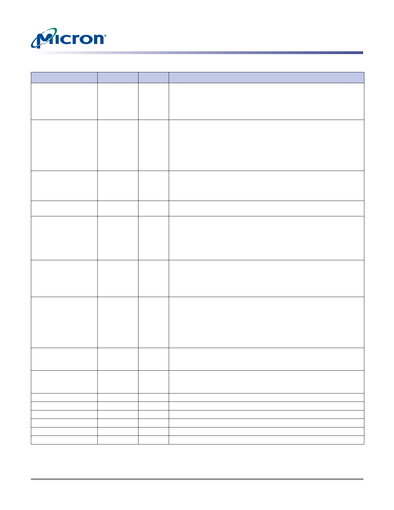
Table 3: 60-Ball VFBGA Ball Descriptions
Ball Numbers
G2, G3
Symbol
CK, CK#
G1
CKE
H7
CS#
G9, G8, G7
F2, F8
RAS#, CAS#,
WE#
UDM, LDM
H8, H9
BA0, BA1
J8, J9, K7, K8, K2, K3,
J1, J2, J3, H1, J7, H2, H3
A0–A12
A8, B7, B8, C7, C8, D7,
D8, E7, E3, D2, D3, C2,
C3, B2, B3, A2
E2, E8
DQ0–DQ15
UDQS, LDQS
A7, B1, C9, D1, E9
A3, B9, C1, E1
A9, F9, K9
A1, F1, K1
F3, F7
D9
VDDQ
VSSQ
VDD
VSS
NC
TEST
Type
Input
Input
Input
Input
Input
Input
Input
I/O
Description
Clock: CK is the system clock input. CK and CK# are differential clock
inputs. All address and control input signals are sampled on the
crossing of the positive edge of CK and the negative edge of CK#.
Input and output data is referenced to the crossing of CK and CK#
(both directions of the crossing).
Clock enable: CKE HIGH activates and CKE LOW deactivates the
internal clock signals, input buffers, and output drivers. Taking CKE
LOW enables PRECHARGE power-down and SELF REFRESH operations
(all banks idle) or ACTIVE power-down (row active in any bank). CKE is
synchronous for all functions except SELF REFRESH exit. All input
buffers (except CKE) are disabled during power-down and self refresh
modes.
Chip select: CS# enables (registered LOW) and disables (registered
HIGH) the command decoder. All commands are masked when CS# is
registered HIGH. CS# provides for external bank selection on systems
with multiple banks. CS# is considered part of the command code.
Command inputs: RAS#, CAS#, and WE# (along with CS#) define the
command being entered.
Input data mask: DM is an input mask signal for write data. Input
data is masked when DM is sampled HIGH along with that input data
during a WRITE access. DM is sampled on both edges of DQS. Although
DM balls are input-only, the DM loading is designed to match that of
DQ and DQS balls. For the x16, LDM is DM for DQ0–DQ7, and UDM is
DM for DQ8–DQ15.
Bank address inputs: BA0 and BA1 define to which bank an ACTIVE,
READ, WRITE, or PRECHARGE command is being applied. BA0 and BA1
also determine which mode register (standard mode register or
extended mode register) is loaded during a LOAD MODE REGISTER
command.
Address inputs: Provide the row address for ACTIVE commands, and
the column address and auto precharge bit (A10) for READ/WRITE
commands, to select one location out of the memory array in the
respective bank. During a PRECHARGE command, A10 determines
whether the PRECHARGE applies to one bank (A10 LOW, bank selected
by BA0, BA1) or all banks (A10 HIGH). The address inputs also provide
the op-code during a LOAD MODE REGISTER command.
Data input/output: Data bus for x16.
I/O
Supply
Supply
Supply
Supply
–
–
Data strobe: Output with read data, input with write data. DQS is
edge-aligned with read data, center-aligned with write data. Data
strobe is used to capture data.
DQ power supply.
DQ ground.
Power supply.
Ground.
No connect: May be left unconnected.
Test pin that must be connected to Vss or VSSQ in normal operation.
PDF: 09005aef82091978 / Source: 09005aef8209195b
MT46H16M16LF__2.fm - Rev. H 6/08 EN
11
Micron Technology, Inc., reserves the right to change products or specifications without notice.
©2005 Micron Technology, Inc. All rights reserved.
Share Link: 